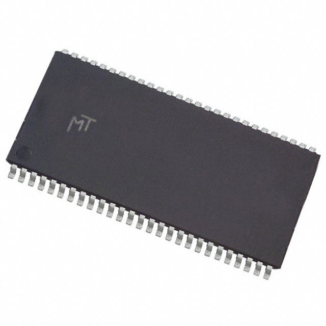
MT48LC64M4A2P-6A:G
| Part Description |
IC DRAM 256MBIT PAR 54TSOP II |
|---|---|
| Quantity | 803 Available (as of June 18, 2026) |

| Product Category | DRAM Memory |
|---|---|
| Manufacturer | Micron Technology Inc. |
| Manufacturing Status | Obsolete |
| Manufacturer Standard Lead Time | Contact Us |
| Datasheet |
Specifications & Environmental
| Device Package | 54-TSOP II | Memory Format | DRAM | Technology | SDRAM | ||
|---|---|---|---|---|---|---|---|
| Memory Size | 256 Mbit | Access Time | 5.4 ns | Grade | Commercial | ||
| Clock Frequency | 167 MHz | Voltage | 3V ~ 3.6V | Memory Type | Volatile | ||
| Operating Temperature | 0°C ~ 70°C (TA) | Write Cycle Time Word Page | 12 ns | Packaging | 54-TSOP (0.400", 10.16mm Width) | ||
| Mounting Method | Volatile | Memory Interface | Parallel | Memory Organization | 64M x 4 | ||
| Moisture Sensitivity Level | 3 (168 Hours) | RoHS Compliance | ROHS3 Compliant | REACH Compliance | REACH Unaffected | ||
| Qualification | N/A | ECCN | EAR99 | HTS Code | 8542.32.0024 |
Overview of MT48LC64M4A2P-6A:G – IC DRAM 256Mbit Parallel, 54‑TSOP II
The MT48LC64M4A2P-6A:G is a 256 Mbit synchronous DRAM (SDRAM) organized as 64M x 4 with a parallel memory interface in a 54-pin TSOP II package. It implements fully synchronous operation with internal pipelined architecture and multiple internal banks to optimize row access and precharge handling.
Designed for systems requiring 256 Mbit of volatile SDRAM at standard 3.3 V supplies, this device offers PC100/PC133 compliance, programmable burst lengths and timing options suited to embedded and system-memory applications where synchronous, high-speed parallel memory is required.
Key Features
- Core Architecture Fully synchronous SDRAM with all signals registered on the positive edge of the system clock and internal pipelined operation for column-address changes every clock cycle.
- Memory Organization 64M × 4 organization (16 Meg × 4 × 4 banks) providing 256 Mbit density with four internal banks for hidden row access and precharge.
- Performance 167 MHz clock frequency (speed grade -6A) with an access time of 5.4 ns and write cycle time (word/page) of 12 ns.
- Timing & Compliance PC100- and PC133-compliant timing options; programmable burst lengths of 1, 2, 4, 8 or full page; CAS latency and RCD/RP timing defined by speed grade.
- Refresh & Power Modes Auto refresh and auto precharge modes supported; self-refresh mode provided (not available on AT devices); 64 ms/8192-cycle refresh for commercial devices per datasheet.
- I/O & Voltage LVTTL-compatible inputs and outputs; single 3.3 V ±0.3 V power supply (3.0 V to 3.6 V listed).
- Package 54-pin TSOP II (0.400", 10.16 mm width) plastic package (standard) optimized for surface-mount assembly.
- Operating Range Commercial operating temperature 0 °C to +70 °C (TA) as specified for this part.
Typical Applications
- PC100/PC133 memory designs Suitable for system designs targeting PC100 or PC133 timing compliance as indicated in the product datasheet.
- Legacy and parallel-memory systems Use where a 54-pin TSOP II packaged 256 Mbit ×4 SDRAM with a parallel interface is required.
- Embedded systems with 3.3 V supply Fits embedded applications operating from a single 3.0–3.6 V supply and within a 0 °C to +70 °C commercial temperature range.
Unique Advantages
- Synchronous pipelined architecture: Enables column address changes every clock cycle and internal bank structure for improved access sequencing.
- Flexible burst and timing options: Programmable burst lengths (1, 2, 4, 8, full page) and defined speed grades (including -6A at 167 MHz) let designers match performance to system timing.
- Standard 3.3 V operation: Single 3.3 V ±0.3 V supply simplifies power design in systems using LVTTL-compatible I/O.
- Compact TSOP II package: 54-pin TSOP II (400 mil) package provides a surface-mount form factor for space-constrained board designs.
- Built-in refresh and power modes: Auto refresh, auto precharge and self-refresh capability (per datasheet) reduce software refresh handling and support low-activity retention.
Why Choose MT48LC64M4A2P-6A:G?
The MT48LC64M4A2P-6A:G positions itself as a straightforward 256 Mbit SDRAM solution for designs that require fully synchronous parallel memory in a compact TSOP II package. Its PC100/PC133-compliant timing options, programmable burst lengths and internal banking provide designers predictable timing and access flexibility for system memory implementations.
This part is suited to customers needing a 64M × 4 SDRAM device that operates from a single 3.3 V supply within a commercial temperature range, and who value a package and timing feature set consistent with established SDRAM system designs.
Request a quote or contact sales to discuss availability, lead times and pricing for MT48LC64M4A2P-6A:G.