MT48LC64M4A2P-75:D TR
| Part Description |
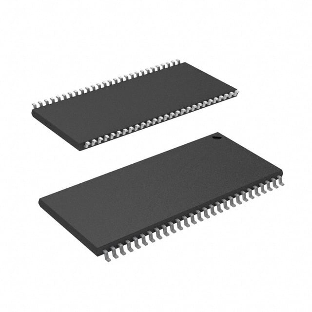
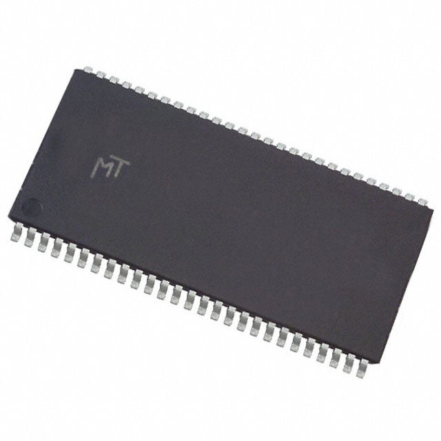
IC DRAM 256MBIT PAR 54TSOP II |
|---|---|
| Quantity | 413 Available (as of June 14, 2026) |

| Product Category | Memory |
|---|---|
| Manufacturer | Micron Technology Inc. |
| Manufacturing Status | Obsolete |
| Manufacturer Standard Lead Time | Contact Us |
| Datasheet |
Specifications & Environmental
| Device Package | 54-TSOP II | Memory Format | DRAM | Technology | SDRAM | ||
|---|---|---|---|---|---|---|---|
| Memory Size | 256 Mbit | Access Time | 5.4 ns | Grade | Commercial | ||
| Clock Frequency | 133 MHz | Voltage | 3V ~ 3.6V | Memory Type | Volatile | ||
| Operating Temperature | 0°C ~ 70°C (TA) | Write Cycle Time Word Page | 15 ns | Packaging | 54-TSOP (0.400", 10.16mm Width) | ||
| Mounting Method | Volatile | Memory Interface | Parallel | Memory Organization | 64M x 4 | ||
| Moisture Sensitivity Level | 3 (168 Hours) | RoHS Compliance | ROHS3 Compliant | REACH Compliance | REACH Unaffected | ||
| Qualification | N/A | ECCN | EAR99 | HTS Code | 8542.32.0024 |
Overview of MT48LC64M4A2P-75:D TR – IC DRAM 256MBIT PAR 54TSOP II
The MT48LC64M4A2P-75:D TR is a 256 Mbit SDRAM organized as 64M × 4 with a parallel memory interface in a 54-pin TSOP II package. It is a fully synchronous DRAM device designed for PC100/PC133-compliant systems and board-level memory applications.
Key electrical and timing characteristics include a clock frequency of 133 MHz, an access time of 5.4 ns, a write cycle time (word/page) of 15 ns, and a supply voltage range of 3.0 V to 3.6 V. The device is specified for operation from 0°C to 70°C.
Key Features
- Memory Core 256 Mbit SDRAM organized as 64M × 4 with 4 internal banks for improved access concurrency and row management.
- Performance & Timing PC100- and PC133-compliant operation with a clock frequency of 133 MHz and an access time of 5.4 ns. Internal pipelined operation allows column address changes every clock cycle.
- Programmable Burst & Access Modes Supports programmable burst lengths (1, 2, 4, 8, or full page) and auto precharge for flexible data transfers and simplified sequencing.
- Refresh & Power Modes Auto refresh and an available self-refresh mode (note: self-refresh not available on AT devices) with standard refresh counts (8K cycles) as documented for commercial devices.
- Interface & Signaling Fully synchronous operation with all signals registered on the positive edge of the system clock and LVTTL-compatible inputs and outputs.
- Power Single-supply operation specified at 3.0 V to 3.6 V (3.3 V ±0.3 V per datasheet), suitable for 3.3 V system environments.
- Package & Mounting 54-pin TSOP II (0.400", 10.16 mm width) plastic package intended for surface-mount board-level integration.
- Operating Range Commercial operating temperature range of 0°C to 70°C.
Typical Applications
- PC100/PC133 memory subsystems – Use in systems requiring PC100 or PC133-compliant SDRAM timing and behavior.
- Board-level memory expansion – Compact 54-pin TSOP II package for designs needing a discrete parallel SDRAM component.
- Embedded systems (commercial) – Memory for commercial-temperature embedded equipment operating between 0°C and 70°C.
Unique Advantages
- Standards-aligned timing: PC100 and PC133 compliance eases integration into systems designed around those timing requirements.
- Synchronous, pipelined operation: Positive-edge-registered signals and pipelined internal architecture allow predictable timing and efficient column accesses.
- Flexible burst modes: Programmable burst lengths and auto precharge reduce controller complexity for varied transfer sizes.
- Compact TSOP II package: 54-pin, 0.400" TSOP II footprint provides a low-profile option for space-constrained PCBs.
- Wide supply tolerance: 3.0 V to 3.6 V rating accommodates 3.3 V ±0.3 V system rails as documented in the datasheet.
- Robust refresh support: Auto refresh and documented refresh cycles (8K) simplify retention management in commercial applications.
Why Choose IC DRAM 256MBIT PAR 54TSOP II?
The MT48LC64M4A2P-75:D TR delivers a 256 Mbit, 64M × 4 SDRAM solution in a compact 54-pin TSOP II package with PC100/PC133-aligned performance, making it suitable for board-level memory implementations that require synchronous, pipelined SDRAM operation. Its documented timing, burst flexibility, and standard refresh modes provide predictable integration for designs targeting 3.3 V systems within the 0°C to 70°C commercial range.
This device is appropriate for engineers and procurement teams specifying discrete SDRAM components where PC100/PC133 timing compatibility, a small TSOP II footprint, and clear electrical and timing specifications are required for clean system integration and long-term maintainability.
Request a quote or submit a pricing and availability inquiry to obtain lead times and volume pricing for the MT48LC64M4A2P-75:D TR.