MT48LC64M8A2P-75 IT:C TR
| Part Description |
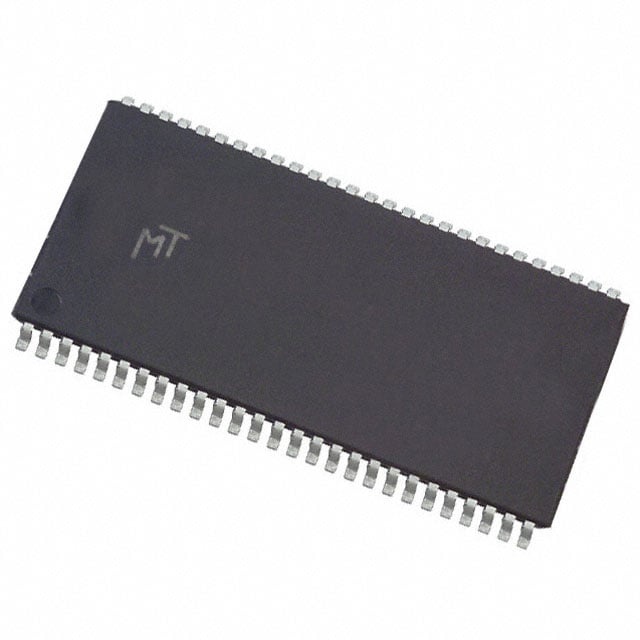
IC DRAM 512MBIT PAR 54TSOP II |
|---|---|
| Quantity | 1,296 Available (as of June 12, 2026) |

| Product Category | Memory |
|---|---|
| Manufacturer | Micron Technology Inc. |
| Manufacturing Status | Obsolete |
| Manufacturer Standard Lead Time | Contact Us |
| Datasheet |
Specifications & Environmental
| Device Package | 54-TSOP II | Memory Format | DRAM | Technology | SDRAM | ||
|---|---|---|---|---|---|---|---|
| Memory Size | 512 Mbit | Access Time | 5.4 ns | Grade | Industrial | ||
| Clock Frequency | 133 MHz | Voltage | 3V ~ 3.6V | Memory Type | Volatile | ||
| Operating Temperature | -40°C ~ 85°C (TA) | Write Cycle Time Word Page | 15 ns | Packaging | 54-TSOP (0.400", 10.16mm Width) | ||
| Mounting Method | Volatile | Memory Interface | Parallel | Memory Organization | 64M x 8 | ||
| Moisture Sensitivity Level | 3 (168 Hours) | RoHS Compliance | ROHS3 Compliant | REACH Compliance | REACH Unaffected | ||
| Qualification | N/A | ECCN | EAR99 | HTS Code | 8542.32.0024 |
Overview of MT48LC64M8A2P-75 IT:C TR – IC DRAM 512MBIT PAR 54TSOP II
The MT48LC64M8A2P-75 IT:C TR is a 512 Mbit SDR SDRAM organized as 64M × 8 with internal bank architecture and a parallel memory interface. It is a fully synchronous DRAM device supporting programmable burst lengths and standard SDRAM control features.
Designed for systems requiring parallel SDRAM memory, this device delivers PC100/PC133-compliant timing, a 133 MHz clock frequency (-75 speed grade), and industrial temperature operation, making it suitable for a range of embedded and system memory applications that require synchronous parallel DRAM.
Key Features
- Memory Architecture 512 Mbit SDRAM organized as 64M × 8 with four internal banks (16 Meg × 8 × 4 banks).
- SDR SDRAM Core Fully synchronous operation with all signals registered on the positive clock edge and internal pipelined operation for column address changes every clock cycle.
- Performance & Timing PC100- and PC133-compliant timing; -75 speed grade supports 133 MHz clock frequency with 5.4 ns access time (CL = 3).
- Programmable Burst & Refresh Programmable burst lengths of 1, 2, 4, 8 or full page. Supports auto refresh and self-refresh with a 64 ms, 8192-cycle refresh period.
- Interface & I/O Parallel memory interface with LVTTL-compatible inputs and outputs for standard SDRAM signal levels.
- Power Single 3.3 V power supply (3.3 V ±0.3 V); specification lists operating supply range of 3.0 V to 3.6 V.
- Timing Parameters Write cycle time (word/page) specified at 15 ns; setup and hold timing consistent with PC100/PC133 timing requirements.
- Package & Temperature 54-pin TSOP II (0.400", 10.16 mm width) package; industrial operating temperature range of –40 °C to +85 °C (TA).
Typical Applications
- Parallel SDRAM memory subsystems Provides 512 Mbit synchronous DRAM in a 54-pin TSOP II package for systems with parallel memory interfaces.
- Embedded systems Supports synchronous system memory implementations requiring PC100/PC133 timing and standard SDRAM control features.
- Legacy and industrial platforms Industrial temperature rating and LVTTL I/O make the device suitable for temperature-sensitive, board-level memory designs.
Unique Advantages
- Industry-standard timing compliance PC100/PC133 compliance ensures predictable timing behavior with established SDRAM system designs.
- Flexible burst control Programmable burst lengths (1, 2, 4, 8, full page) enable tuning for sequential or random-access workload patterns.
- Robust thermal range –40 °C to +85 °C operating range supports deployment in industrial and temperature-variable environments.
- Compact TSOP II package 54-pin TSOP II (400 mil) package provides a compact footprint for high-density board layouts.
- Standard 3.3 V supply Single 3.3 V (3.0–3.6 V) supply simplifies power rail design in systems using conventional SDRAM voltages.
- Self-refresh and auto-refresh support On-device refresh modes reduce external refresh management and help preserve data during low-power or idle states.
Why Choose IC DRAM 512MBIT PAR 54TSOP II?
The MT48LC64M8A2P-75 IT:C TR offers a practical combination of synchronous SDRAM features, PC100/PC133-compliant timing, and industrial temperature operation in a 54-pin TSOP II package. Its 64M × 8 organization with four internal banks and programmable burst capabilities provide predictable performance for parallel memory implementations.
This device is well suited for designers and procurement teams specifying synchronous parallel DRAM for embedded systems, legacy platforms, and industrial applications where 3.3 V supply compatibility, compact package size, and established SDRAM timing are required.
If you would like pricing, availability, or to request a quote for the MT48LC64M8A2P-75 IT:C TR, please submit a quote request or contact sales for more information.