MT48LC64M8A2P-75 IT:C
| Part Description |
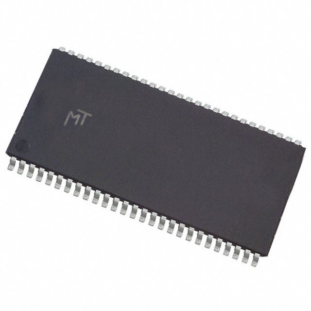
IC DRAM 512MBIT PAR 54TSOP II |
|---|---|
| Quantity | 367 Available (as of June 15, 2026) |

| Product Category | DRAM Memory |
|---|---|
| Manufacturer | Micron Technology Inc. |
| Manufacturing Status | Obsolete |
| Manufacturer Standard Lead Time | Contact Us |
| Datasheet |
Specifications & Environmental
| Device Package | 54-TSOP II | Memory Format | DRAM | Technology | SDRAM | ||
|---|---|---|---|---|---|---|---|
| Memory Size | 512 Mbit | Access Time | 5.4 ns | Grade | Industrial | ||
| Clock Frequency | 133 MHz | Voltage | 3V ~ 3.6V | Memory Type | Volatile | ||
| Operating Temperature | -40°C ~ 85°C (TA) | Write Cycle Time Word Page | 15 ns | Packaging | 54-TSOP (0.400", 10.16mm Width) | ||
| Mounting Method | Volatile | Memory Interface | Parallel | Memory Organization | 64M x 8 | ||
| Moisture Sensitivity Level | 3 (168 Hours) | RoHS Compliance | ROHS Compliant | REACH Compliance | REACH Unaffected | ||
| Qualification | N/A | ECCN | EAR99 | HTS Code | 8542.32.0024 |
Overview of MT48LC64M8A2P-75 IT:C – IC DRAM 512MBIT PAR 54TSOP II
The MT48LC64M8A2P-75 IT:C is a 512 Mbit synchronous DRAM (SDRAM) device organized as 64M × 8 with a parallel memory interface and packaged in a 54-pin TSOP II (400 mil). It implements fully synchronous, pipelined SDRAM architecture with internal banks and programmable burst lengths to support deterministic, clocked memory access.
Its combination of PC100/PC133 timing options, 133 MHz clock support, and industrial temperature range make it suitable for designs that require predictable SDRAM performance in 3.0–3.6 V systems and a compact TSOP II package.
Key Features
- Core / Memory Architecture 512 Mbit SDRAM organized as 64M × 8 with internal bank architecture (4 banks) to enable pipelined operation and reduced row-access overhead.
- Performance & Timing PC100- and PC133-compliant timing with support for up to 133 MHz system clock; typical access time listed as 5.4 ns for the -75 speed grade at CL = 3.
- Programmable Burst & Operation Modes Programmable burst lengths (1, 2, 4, 8, or full-page), auto precharge, concurrent auto precharge/auto refresh modes, and self-refresh for flexible memory sequencing and refresh management.
- Refresh Supports 64 ms, 8192-cycle refresh for standard commercial and industrial refresh timing.
- Signal & I/O Compatibility LVTTL-compatible inputs and outputs with fully synchronous operation—signals registered on the positive edge of the system clock.
- Power Single 3.3 V ±0.3 V power supply (3.0–3.6 V) suitable for standard 3.3 V SDRAM systems.
- Package & Mounting 54-pin TSOP II (0.400", 10.16 mm width) package (54-TSOP II) for surface-mount applications requiring a compact footprint.
- Operating Temperature Industrial temperature range: –40°C to +85°C (TA), indicated by the IT marking.
Typical Applications
- System Memory for Parallel SDRAM Designs Acts as synchronous parallel DRAM in systems that require standard PC100/PC133 SDRAM timing and predictable, pipelined access.
- Embedded and Industrial Electronics Industrial temperature rating (–40°C to +85°C) and standard 3.3 V operation make it suitable for embedded controllers and industrial equipment with parallel memory interfaces.
- Legacy and Performance-Oriented Platforms Provides PC100/PC133-compliant SDRAM capacity and timing for designs that use CL = 3 timing and 133 MHz clocking.
Unique Advantages
- Deterministic, Clocked Operation: Fully synchronous design with all signals registered on the positive edge of the system clock simplifies timing analysis and system integration.
- Flexible Burst and Bank Management: Programmable burst lengths and internal bank architecture allow designers to tune throughput and latency to application needs.
- Industrial Temperature Support: –40°C to +85°C rating enables deployment in temperature-challenging environments without additional thermal qualification data.
- Standard 3.3 V Supply Compatibility: Operates across 3.0–3.6 V, matching common 3.3 V system rails and easing power-supply integration.
- Compact Surface-Mount Package: 54-pin TSOP II footprint provides a space-efficient form factor for PCB designs requiring moderate-density SDRAM.
Why Choose MT48LC64M8A2P-75 IT:C?
The MT48LC64M8A2P-75 IT:C delivers a straightforward 512 Mbit SDRAM option for parallel-memory designs that require PC100/PC133-compatible timing, programmable burst operation, and industrial temperature range. Its fully synchronous, pipelined architecture and LVTTL-compatible I/O provide predictable timing and straightforward integration into 3.3 V systems.
This device is appropriate for designers seeking a compact TSOP II packaged SDRAM with standard refresh and self-refresh capabilities, flexible burst lengths, and support for up to 133 MHz clocking. It is suited to systems where deterministic SDRAM behavior and industrial temperature operation are primary concerns.
If you need pricing, lead-time, or availability information for MT48LC64M8A2P-75 IT:C, request a quote or contact sales to submit a quote request.