
MT48LC8M16A2B4-6A:L
| Part Description |
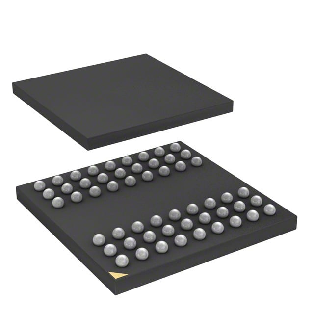
IC DRAM 128MBIT PAR 54VFBGA |
|---|---|
| Quantity | 312 Available (as of June 18, 2026) |
| Product Category | DRAM Memory |
|---|---|
| Manufacturer | Micron Technology Inc. |
| Manufacturing Status | Obsolete |
| Manufacturer Standard Lead Time | Contact Us |
| Datasheet |
Specifications & Environmental
| Device Package | 54-VFBGA (8x8) | Memory Format | DRAM | Technology | SDRAM | ||
|---|---|---|---|---|---|---|---|
| Memory Size | 128 Mbit | Access Time | 5.4 ns | Grade | Commercial | ||
| Clock Frequency | 167 MHz | Voltage | 3V ~ 3.6V | Memory Type | Volatile | ||
| Operating Temperature | 0°C ~ 70°C (TA) | Write Cycle Time Word Page | 12 ns | Packaging | 54-VFBGA | ||
| Mounting Method | Volatile | Memory Interface | Parallel | Memory Organization | 8M x 16 | ||
| Moisture Sensitivity Level | 3 (168 Hours) | RoHS Compliance | ROHS3 Compliant | REACH Compliance | REACH Unaffected | ||
| Qualification | N/A | ECCN | EAR99 | HTS Code | 8542.32.0002 |
Overview of MT48LC8M16A2B4-6A:L – IC DRAM 128Mbit PAR 54VFBGA
The MT48LC8M16A2B4-6A:L is a 128 Mbit synchronous DRAM organized as 8M × 16 with a parallel memory interface in a 54-ball VFBGA (8×8) package. It implements fully synchronous SDRAM architecture with internal banks, programmable burst lengths and support for auto refresh and self-refresh modes.
This device is intended for systems that require a 128 Mbit parallel SDRAM solution with a +3.3 V supply range and commercial-temperature operation. It provides fixed-timing performance options including a -6A speed grade with up to 167 MHz clock support and 5.4 ns access timing where specified.
Key Features
- Core / Architecture Fully synchronous SDRAM with all signals registered on the positive edge of the system clock and internal pipelined operation.
- Memory Organization 128 Mbit capacity organized as 8M × 16 with 4 internal banks (2 Meg × 16 × 4 banks as referenced in datasheet).
- Performance Supports a -6A speed grade (listed clock frequency 167 MHz) and has an access time of 5.4 ns in the documented timing table.
- Timing & Burst Programmable burst lengths (1, 2, 4, 8, or full page) and internal bank architecture that hides row access/precharge. Write cycle time (word/page) is 12 ns.
- Refresh & Self-Refresh Auto Refresh modes and a 64 ms, 4,096-cycle refresh specification; self-refresh available with a low-power option (designation “L” for low power self-refresh in the datasheet options).
- Interface & I/O Parallel memory interface with LVTTL-compatible inputs and outputs; all signals synchronous to clock.
- Power Single supply operation at +3.3 V nominal (documented voltage range 3.0 V to 3.6 V).
- Package & Temperature 54-ball VFBGA (8×8) package; commercial operating temperature range 0°C to +70°C (TA).
- Standards PC100- and PC133-compliant options are listed in the product datasheet.
Typical Applications
- Parallel memory subsystems Acts as a 128 Mbit parallel SDRAM device for designs that integrate parallel synchronous DRAM.
- Embedded platforms Provides synchronous DRAM storage where a 3.3 V parallel memory interface and a 54-ball VFBGA package are required.
- Legacy SDRAM designs Suitable for systems using PC100/PC133-compatible SDRAM timing options as documented in the datasheet.
Unique Advantages
- Synchronous, pipelined architecture: Internal pipelined operation and registered inputs enable column-address changes every clock cycle for deterministic timing.
- Flexible burst control: Programmable burst lengths from 1 to full page allow tailoring transfers to system access patterns.
- Refresh robustness: 64 ms / 4,096-cycle refresh specification with auto and self-refresh modes for maintaining data integrity during refresh intervals.
- Documented performance grade: -6A speed grade with listed 167 MHz clock frequency and 5.4 ns access timing in the datasheet for timing-critical designs.
- Standard voltage and I/O compatibility: Operates from 3.0 V to 3.6 V and uses LVTTL-compatible inputs/outputs for straightforward interface design.
- Compact BGA package: 54-ball VFBGA (8×8) package reduces board footprint while providing the necessary ballout for parallel memory connections.
Why Choose IC DRAM 128MBIT PAR 54VFBGA?
The MT48LC8M16A2B4-6A:L delivers a documented 128 Mbit parallel SDRAM solution with synchronous, pipelined operation and flexible burst and refresh modes. Its combination of an 8M × 16 organization, -6A timing grade, and LVTTL I/O support makes it suitable for designs that require predictable SDRAM timing and a 3.3 V supply.
This device is positioned for commercial-temperature applications (0°C to +70°C) that need a compact 54-ball VFBGA package and PC100/PC133-compatible timing options as described in the manufacturer datasheet. The inclusion of auto and self-refresh modes and a low-power self-refresh option adds operational flexibility for a range of system requirements.
Request a quote or submit a request for a formal quotation to evaluate the MT48LC8M16A2B4-6A:L for your next SDRAM design requirement.


