MT48LC8M16A2P-7E:L
| Part Description |
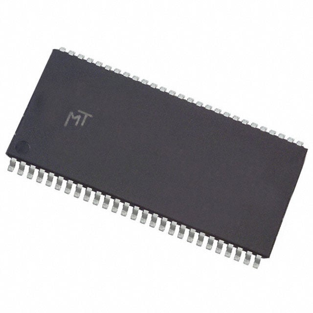
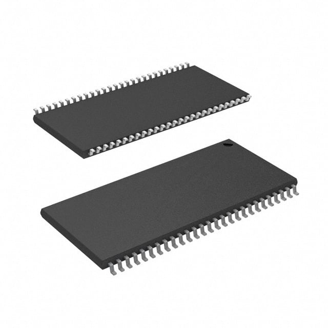
IC DRAM 128MBIT PAR 54TSOP II |
|---|---|
| Quantity | 512 Available (as of June 9, 2026) |

| Product Category | Memory |
|---|---|
| Manufacturer | Micron Technology Inc. |
| Manufacturing Status | Obsolete |
| Manufacturer Standard Lead Time | Contact Us |
| Datasheet |
Specifications & Environmental
| Device Package | 54-TSOP II | Memory Format | DRAM | Technology | SDRAM | ||
|---|---|---|---|---|---|---|---|
| Memory Size | 128 Mbit | Access Time | 5.4 ns | Grade | Commercial | ||
| Clock Frequency | 133 MHz | Voltage | 3V ~ 3.6V | Memory Type | Volatile | ||
| Operating Temperature | 0°C ~ 70°C (TA) | Write Cycle Time Word Page | 14 ns | Packaging | 54-TSOP (0.400", 10.16mm Width) | ||
| Mounting Method | Volatile | Memory Interface | Parallel | Memory Organization | 8M x 16 | ||
| Moisture Sensitivity Level | 3 (168 Hours) | RoHS Compliance | ROHS3 Compliant | REACH Compliance | REACH Unaffected | ||
| Qualification | N/A | ECCN | EAR99 | HTS Code | 8542.32.0002 |
Overview of MT48LC8M16A2P-7E:L – IC DRAM 128MBIT PAR 54TSOP II
The MT48LC8M16A2P-7E:L is a 128 Mbit synchronous DRAM (SDRAM) device organized as 8M × 16 with a parallel memory interface. It implements a fully synchronous, pipelined SDRAM architecture with internal banks, programmable burst lengths and multiple refresh and self-refresh modes.
This device targets commercial-temperature designs that require PC100/PC133-class SDRAM timing, a 3.3 V supply range, and a 54-pin TSOP II footprint for compact board-level integration.
Key Features
- Core / Memory Architecture Fully synchronous SDRAM with internal pipelined operation and multiple internal banks to help hide row access and precharge latency.
- Memory Capacity & Organization 128 Mbit memory organized as 8M × 16, implemented as synchronous DRAM for parallel-system integration.
- Performance & Timing PC100 and PC133 compliant timing options; typical clock frequency listed at 133 MHz with a 5.4 ns access time and 14 ns write cycle time (word/page).
- Programmable Transfer Modes Supports programmable burst lengths (1, 2, 4, 8, or full page), Auto Precharge (including concurrent Auto Precharge), Auto Refresh and Self Refresh modes.
- Signal Compatibility LVTTL-compatible inputs and outputs; all signals are registered on the positive edge of the system clock.
- Power Single-supply operation with a listed voltage range of 3.0 V to 3.6 V (documented as +3.3 V ±0.3 V in product literature).
- Refresh Standard 64 ms, 4,096-cycle refresh sequence supported to maintain stored data integrity.
- Package & Temperature 54-pin TSOP II (0.400", 10.16 mm width) package; commercial operating temperature range 0 °C to +70 °C.
Typical Applications
- Commercial Embedded Systems Off-board SDRAM for compact embedded designs operating at commercial temperatures that require parallel SDRAM capacity and timing.
- PC100 / PC133-Class Memory Subsystems Use in legacy or specialized platforms that require PC100/PC133-compliant SDRAM timing and behavior.
- Board-Level Memory Expansion 54-pin TSOP II footprint enables board-level integration where a 128 Mbit parallel SDRAM device is required for system buffers or working memory.
Unique Advantages
- PC100/PC133 Compliance: Documented timing grades and PC100/PC133 compliance simplify integration into systems targeting those clock domains.
- Pipelined, Banked Architecture: Internal pipelining and multiple banks allow column address changes every clock cycle and reduce effective latency for burst transfers.
- Flexible Burst and Refresh Modes: Programmable burst lengths plus Auto Precharge, Auto Refresh and Self Refresh provide flexibility for diverse memory access patterns and power scenarios.
- Industry-Standard Voltage and I/O: Single-supply 3.0–3.6 V operation with LVTTL-compatible I/O supports common system voltage rails and signaling.
- Compact Package: 54-pin TSOP II (0.400") package offers a space-efficient footprint for board-level memory implementations.
Why Choose IC DRAM 128MBIT PAR 54TSOP II?
The MT48LC8M16A2P-7E:L combines a 128 Mbit SDRAM organization with PC100/PC133-class timing, a 54-pin TSOP II package and a standard 3.3 V supply range to address commercial designs that need parallel SDRAM capacity with predictable timing. Its fully synchronous, pipelined architecture and internal bank structure provide the control and transfer flexibility required for burst-oriented memory systems.
This device is suitable for designers specifying a compact, commercial-temperature SDRAM solution with documented access times, clock-frequency grades and refresh behavior. Use it where a proven Micron SDRAM family device is required for system memory, buffering or legacy platform support.
Request a quote or contact sales for pricing, availability and lead-time information for MT48LC8M16A2P-7E:L. Provide the full part number when submitting inquiries for the fastest response.