MT48LC8M16A2TG-75 IT:G TR
| Part Description |
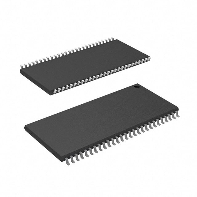
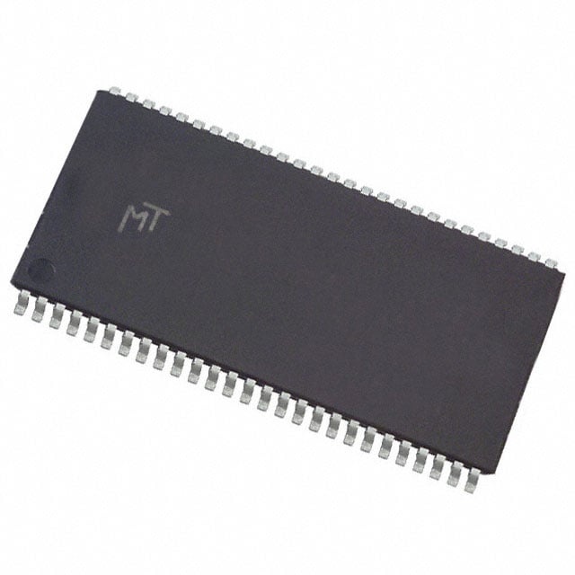
IC DRAM 128MBIT PAR 54TSOP II |
|---|---|
| Quantity | 1,054 Available (as of June 14, 2026) |

| Product Category | Memory |
|---|---|
| Manufacturer | Micron Technology Inc. |
| Manufacturing Status | Obsolete |
| Manufacturer Standard Lead Time | Contact Us |
| Datasheet |
Specifications & Environmental
| Device Package | 54-TSOP II | Memory Format | DRAM | Technology | SDRAM | ||
|---|---|---|---|---|---|---|---|
| Memory Size | 128 Mbit | Access Time | 5.4 ns | Grade | Industrial | ||
| Clock Frequency | 133 MHz | Voltage | 3V ~ 3.6V | Memory Type | Volatile | ||
| Operating Temperature | -40°C ~ 85°C (TA) | Write Cycle Time Word Page | 15 ns | Packaging | 54-TSOP (0.400", 10.16mm Width) | ||
| Mounting Method | Volatile | Memory Interface | Parallel | Memory Organization | 8M x 16 | ||
| Moisture Sensitivity Level | 3 (168 Hours) | RoHS Compliance | RoHS non-compliant | REACH Compliance | REACH Unaffected | ||
| Qualification | N/A | ECCN | EAR99 | HTS Code | 8542.32.0002 |
Overview of MT48LC8M16A2TG-75 IT:G TR – IC DRAM 128MBIT PAR 54TSOP II
The MT48LC8M16A2TG-75 IT:G TR is a 128 Mbit SDRAM organized as 8M × 16 with a parallel memory interface in a 54‑pin TSOP II package. It implements fully synchronous SDR SDRAM architecture and is targeted at systems requiring PC100/PC133‑class synchronous DRAM performance with industrial temperature operation.
Key operational characteristics include a 133 MHz clock frequency, 3.0 V–3.6 V single supply, fast access times, internal pipelined operation and internal bank architecture to support efficient burst and pipelined memory access patterns.
Key Features
- Core / Architecture Fully synchronous SDR SDRAM organized as 8M × 16 with four internal banks to support pipelined operation and concurrent row access/precharge handling.
- Memory Capacity & Organization 128 Mbit total capacity presented as 8M × 16, suitable for parallel DRAM memory subsystems.
- Performance PC100‑ and PC133‑compliant timing options with a clock frequency of 133 MHz and an access time specified at 5.4 ns. Programmable burst lengths (1, 2, 4, 8, or full page).
- Timing and Cycle Target timing grades include 3‑3‑3 and 2‑2‑2 CAS latencies; write cycle time (word/page) is 15 ns for the specified device.
- Power Single 3.3 V ±0.3 V supply range (3.0 V–3.6 V) with standard and low‑power self‑refresh modes noted in device options.
- Interfaces & I/O LVTTL‑compatible inputs and outputs with all signals registered on the positive edge of the system clock to maintain synchronous operation.
- System Reliability Auto refresh (4K cycle refresh), auto precharge and selectable refresh modes to maintain data integrity during normal and low‑power operation.
- Package & Temperature 54‑pin TSOP II (400 mil, 10.16 mm width) plastic package with industrial operating temperature range of –40°C to +85°C.
Typical Applications
- Industrial Control Systems Provides synchronous parallel DRAM capacity for control and data buffering in equipment operating across –40°C to +85°C.
- Embedded Memory Subsystems Acts as a compact SDRAM device for embedded boards requiring PC100/PC133 timing and a 54‑pin TSOP II footprint.
- System Memory Buffers Supports high‑rate burst transfers and pipelined access patterns for buffer and working memory roles in electronic systems.
Unique Advantages
- Industry‑standard timing compatibility: PC100 and PC133 compliance ensures predictable integration into systems designed around these SDRAM timing classes.
- High‑speed synchronous operation: 133 MHz clock frequency and programmable CAS latency options enable flexible performance tuning for target system requirements.
- Industrial temperature rating: –40°C to +85°C operation supports deployment in temperature‑challenging environments.
- Compact TSOP II packaging: 54‑pin TSOP II (0.400", 10.16 mm width) provides a dense, board‑level footprint for space‑constrained designs.
- Single 3.3 V supply: 3.0 V–3.6 V operation simplifies power rail design while supporting standard LVTTL I/O levels.
- Built‑in refresh and power features: Auto refresh, auto precharge and self‑refresh options help maintain data integrity and support low‑power modes.
Why Choose MT48LC8M16A2TG-75 IT:G TR?
The MT48LC8M16A2TG-75 IT:G TR delivers a compact 128 Mbit SDRAM solution with PC100/PC133 synchronous operation, flexible timing options and industrial temperature capability. Its 8M × 16 organization, internal pipelined banks and programmable burst lengths make it suitable for systems that require predictable parallel SDRAM performance and efficient burst transfers.
This device is appropriate for designers seeking a proven SDRAM building block in a 54‑pin TSOP II package, supporting 3.3 V supply systems and operating across extended temperature ranges for robust field deployment.
Request a quote or submit a request for pricing and availability to get more information and lead‑time for the MT48LC8M16A2TG-75 IT:G TR.