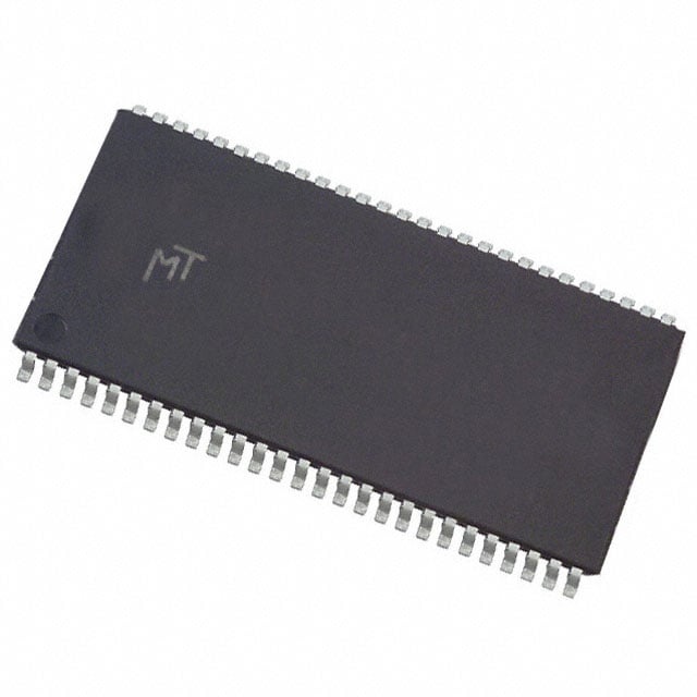
MT48LC8M16A2TG-75 L IT:G
| Part Description |
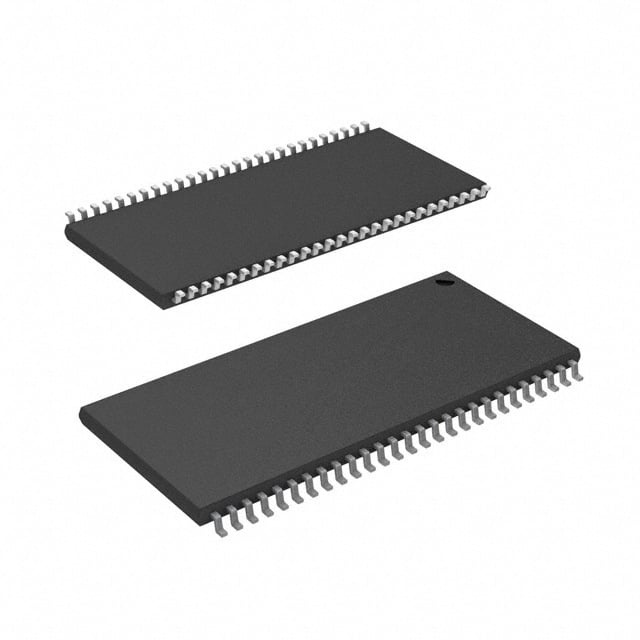
IC DRAM 128MBIT PAR 54TSOP II |
|---|---|
| Quantity | 419 Available (as of June 14, 2026) |

| Product Category | Memory |
|---|---|
| Manufacturer | Micron Technology Inc. |
| Manufacturing Status | Obsolete |
| Manufacturer Standard Lead Time | Contact Us |
| Datasheet |
Specifications & Environmental
| Device Package | 54-TSOP II | Memory Format | DRAM | Technology | SDRAM | ||
|---|---|---|---|---|---|---|---|
| Memory Size | 128 Mbit | Access Time | 5.4 ns | Grade | Industrial | ||
| Clock Frequency | 133 MHz | Voltage | 3V ~ 3.6V | Memory Type | Volatile | ||
| Operating Temperature | -40°C ~ 85°C (TA) | Write Cycle Time Word Page | 15 ns | Packaging | 54-TSOP (0.400", 10.16mm Width) | ||
| Mounting Method | Volatile | Memory Interface | Parallel | Memory Organization | 8M x 16 | ||
| Moisture Sensitivity Level | 2 (1 Year) | RoHS Compliance | N/A | REACH Compliance | REACH Unaffected | ||
| Qualification | N/A | ECCN | EAR99 | HTS Code | 8542.32.0002 |
Overview of MT48LC8M16A2TG-75 L IT:G – IC DRAM 128MBIT PAR 54TSOP II
The MT48LC8M16A2TG-75 L IT:G is a 128 Mbit synchronous DRAM (SDRAM) device from Micron Technology Inc. Organized as 8M × 16 with four internal banks, it implements a fully synchronous, pipelined SDRAM architecture for parallel system memory applications.
Targeted at PC100/PC133-class systems and industrial embedded designs, this device delivers 133 MHz operation with programmable burst lengths and standard SDRAM command features to support high-throughput buffering and system memory tasks across a wide operating temperature range.
Key Features
- Core / Architecture Organized as 8M × 16 with four internal banks (2M × 16 per bank) to support banked row access and internal precharge.
- Memory Type & Format SDR SDRAM, volatile DRAM in a parallel memory interface format.
- Performance PC100- and PC133-compliant; clock frequency rated at 133 MHz and supporting fully synchronous, pipelined operation with column address changes every clock cycle.
- Programmable Burst & Access Modes Programmable burst lengths (1, 2, 4, 8, or full page), auto precharge, auto refresh and self-refresh modes (standard and low power noted in datasheet).
- Timing Access time listed at 5.4 ns and write cycle time (word/page) of 15 ns; speed-grade information and CAS timing options are provided in the device datasheet.
- Voltage & Power Single-supply operation from 3.0 V to 3.6 V.
- Package & Mounting 54-pin TSOP II (0.400", 10.16 mm width) plastic package for board-level mounting.
- Operating Temperature Industrial temperature range: –40 °C to +85 °C (TA).
Typical Applications
- PC-class memory subsystems Suitable for PC100/PC133-class systems requiring standard SDRAM buffering and synchronous parallel memory.
- Industrial embedded systems Extended temperature range enables use in industrial controllers, data acquisition modules, and other embedded equipment operating between –40 °C and +85 °C.
- High-throughput buffering Pipelined SDRAM operation and programmable burst lengths support buffering and temporary storage in systems with parallel memory interfaces.
Unique Advantages
- Banked memory organization: Internal four-bank structure helps hide row access/precharge and supports efficient pipelined operation.
- PC100/PC133 compliance: Clock-rate and timing options align with PC100/PC133-class system requirements for straightforward integration into legacy parallel SDRAM designs.
- Industrial temperature rating: –40 °C to +85 °C operating range supports deployment in harsh or temperature-variable environments.
- Compact TSOP II package: 54-pin, 0.400" (10.16 mm) TSOP II package offers a small board footprint for space-constrained designs.
- Flexible timing and burst options: Programmable burst lengths and standard SDRAM refresh/precharge modes provide designers control over throughput and memory access patterns.
- Single 3.3 V supply: Standard 3.0–3.6 V supply simplifies power-rail requirements for systems using 3.3 V logic domains.
Why Choose IC DRAM 128MBIT PAR 54TSOP II?
The MT48LC8M16A2TG-75 L IT:G provides a straightforward, industry-recognized SDRAM building block for parallel memory applications that require PC100/PC133-class timing, banked memory access and an industrial temperature range. Its combination of 8M × 16 organization, programmable burst modes and compact 54-pin TSOP II packaging makes it suitable for embedded designs where established SDRAM behavior and predictable timing are required.
This device is appropriate for designers and procurement teams specifying synchronous DRAM for legacy parallel interfaces or industrial applications that demand robust temperature performance and standard 3.3 V supply operation. Detailed timing and option information is published in the device datasheet for design verification and system integration.
Request a quote or submit an inquiry to obtain pricing and lead-time information for the MT48LC8M16A2TG-75 L IT:G.