MT48LC8M32B2P-7 TR
| Part Description |
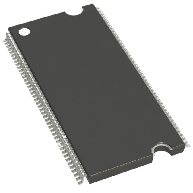
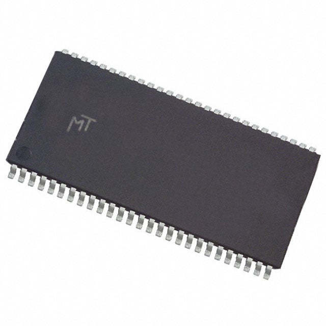
IC DRAM 256MBIT PAR 86TSOP II |
|---|---|
| Quantity | 777 Available (as of June 14, 2026) |

| Product Category | Memory |
|---|---|
| Manufacturer | Micron Technology Inc. |
| Manufacturing Status | Obsolete |
| Manufacturer Standard Lead Time | Contact Us |
| Datasheet |
Specifications & Environmental
| Device Package | 86-TSOP II | Memory Format | DRAM | Technology | SDRAM | ||
|---|---|---|---|---|---|---|---|
| Memory Size | 256 Mbit | Access Time | 6 ns | Grade | Commercial | ||
| Clock Frequency | 143 MHz | Voltage | 3V ~ 3.6V | Memory Type | Volatile | ||
| Operating Temperature | 0°C ~ 70°C (TA) | Write Cycle Time Word Page | 14 ns | Packaging | 86-TFSOP (0.400", 10.16mm Width) | ||
| Mounting Method | Volatile | Memory Interface | Parallel | Memory Organization | 8M x 32 | ||
| Moisture Sensitivity Level | 2 (1 Year) | RoHS Compliance | ROHS Compliant | REACH Compliance | REACH Unaffected | ||
| Qualification | N/A | ECCN | EAR99 | HTS Code | 8542.32.0024 |
Overview of MT48LC8M32B2P-7 TR – IC DRAM 256MBIT PAR 86TSOP II
The MT48LC8M32B2P-7 TR is a 256 Mbit synchronous DRAM organized as 8M × 32 with a parallel memory interface. It is a fully synchronous SDRAM device designed for systems requiring PC100 functionality and standard +3.3 V operation.
Key attributes include a 143 MHz clock rate (speed grade -7), 6.0 ns access time at CAS latency = 3, programmable burst lengths, and an 86-pin TSOP II (400 mil / 10.16 mm width) package for surface-mount applications. The device operates over a commercial temperature range of 0°C to +70°C and supports JEDEC-style refresh and power management modes documented in the datasheet.
Key Features
- Core / Architecture 8M × 32 organization (2 Meg × 32 × 4 banks) with internal banks to hide row access and precharge latency.
- Synchronous SDRAM Fully synchronous operation with all signals registered on the positive edge of the system clock and internal pipelined operation allowing column address changes every clock cycle.
- Performance / Timing Speed grade -7: 143 MHz clock frequency and 6.0 ns access time (CAS latency = 3). Supports CAS latencies of 1, 2, and 3 and programmable burst lengths of 1, 2, 4, 8, or full page.
- Refresh & Power Modes Auto Refresh (4,096-cycle refresh / 64 ms), Self Refresh mode, Auto Precharge and Concurrent Auto Precharge options for standard SDRAM refresh and power-management sequences.
- Interface / I/O Parallel memory interface with LVTTL-compatible inputs and outputs; supports PC100 functionality.
- Power Single-supply operation at +3.3 V ±0.3 V (3.0 V to 3.6 V).
- Package 86-pin TSOP II (400 mil / 10.16 mm width) surface-mount package suitable for high-density PCB assembly.
- Operating Range Commercial temperature range: 0°C to +70°C (TA).
- Write Cycle Write cycle time (word/page): 14 ns as specified in the device data.
Typical Applications
- Parallel SDRAM Memory Subsystem — Provides 256 Mbit of synchronous parallel DRAM storage for systems requiring PC100-compatible memory and standard +3.3 V operation.
- Buffered/High-throughput Data Buffers — 8M × 32 organization with internal pipelining and programmable burst lengths for burst-oriented read/write operations.
- Systems Requiring Standard SDRAM Control — Supports standard SDRAM commands (AUTO REFRESH, SELF REFRESH, AUTO PRECHARGE) and CAS latency settings for conventional memory controller implementations.
Unique Advantages
- Defined speed grade (-7) and timing: 143 MHz clock and 6.0 ns access time provide a clear performance profile for system timing closure.
- Flexible burst and latency options: Programmable burst lengths and CAS latency settings (1, 2, 3) let designers tune throughput and latency for target workloads.
- Integrated bank architecture: Four internal banks enable overlapping row activation and precharge to improve effective access efficiency.
- Standard +3.3 V single-supply operation: Simplifies power-rail design by operating across 3.0 V to 3.6 V tolerances.
- Comprehensive refresh and power modes: Auto Refresh, Self Refresh, and Auto Precharge features support standard SDRAM refresh management and power control.
- Surface-mount TSOP II package: 86-pin TSOP (400 mil / 10.16 mm) provides a compact footprint for high-density PCB layouts.
Why Choose MT48LC8M32B2P-7 TR?
The MT48LC8M32B2P-7 TR is positioned for designs requiring a documented PC100-compatible synchronous parallel memory device with a defined 143 MHz / 6 ns (-7) timing specification. Its 8M × 32 organization, internal banking, and programmable burst/latency options make it suitable for systems that implement conventional SDRAM control and require predictable timing for memory subsystems.
With single-supply +3.3 V operation and an 86-pin TSOP II surface-mount package, the device fits into standard PCB power and mechanical designs while providing refresh and power-management modes necessary for sustained operation and low-power standby scenarios documented in the datasheet.
Request a quote or contact sales to obtain pricing, lead-time, or sample information for the MT48LC8M32B2P-7 TR.