MT48LC8M32B2F5-7 IT TR
| Part Description |
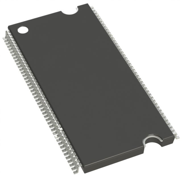
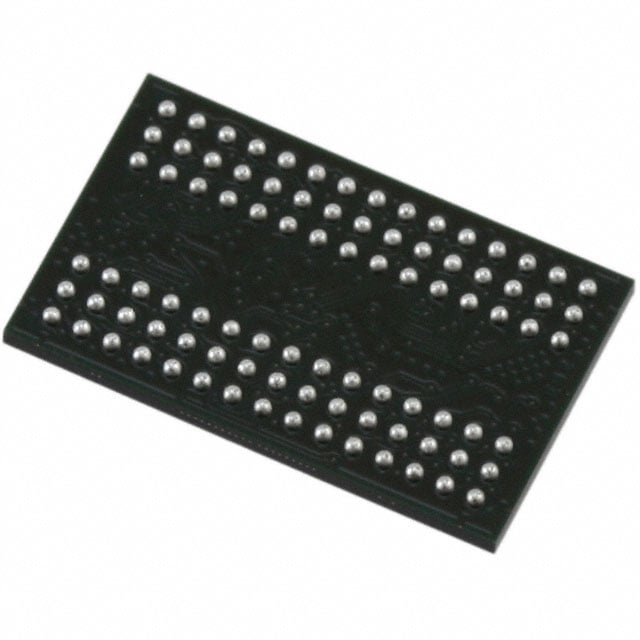
IC DRAM 256MBIT PAR 90VFBGA |
|---|---|
| Quantity | 1,125 Available (as of June 17, 2026) |
| Product Category | DRAM Memory |
|---|---|
| Manufacturer | Micron Technology Inc. |
| Manufacturing Status | Obsolete |
| Manufacturer Standard Lead Time | Contact Us |
| Datasheet |
Specifications & Environmental
| Device Package | 90-VFBGA (8x13) | Memory Format | DRAM | Technology | SDRAM | ||
|---|---|---|---|---|---|---|---|
| Memory Size | 256 Mbit | Access Time | 6 ns | Grade | Industrial | ||
| Clock Frequency | 143 MHz | Voltage | 3V ~ 3.6V | Memory Type | Volatile | ||
| Operating Temperature | -40°C ~ 85°C (TA) | Write Cycle Time Word Page | 14 ns | Packaging | 90-VFBGA | ||
| Mounting Method | Volatile | Memory Interface | Parallel | Memory Organization | 8M x 32 | ||
| Moisture Sensitivity Level | 2 (1 Year) | RoHS Compliance | RoHS non-compliant | REACH Compliance | REACH Unaffected | ||
| Qualification | N/A | ECCN | EAR99 | HTS Code | 8542.32.0024 |
Overview of MT48LC8M32B2F5-7 IT TR – IC DRAM 256MBIT PAR 90VFBGA
The MT48LC8M32B2F5-7 IT TR is a 256 Mbit synchronous DRAM organized as 8M × 32 with a parallel interface in a 90-ball VFBGA (8 mm × 13 mm) package. It implements fully synchronous, pipelined SDRAM architecture with internal banks and features targeted timing for 143 MHz operation (–7 speed grade) with a 6 ns access time at CL = 3.
Designed for systems that require a 256 Mbit parallel SDRAM device with industrial temperature capability, this Micron device supports programmable burst lengths, auto-refresh and self-refresh modes, and operates from a single +3.3 V ±0.3 V supply.
Key Features
- Core / Architecture Fully synchronous SDRAM with internal pipelined operation and internal banks (2M × 32 × 4 banks) for efficient row access and precharge management.
- Memory Organization 8M × 32 organization delivering 256 Mbit total capacity with a 32-bit data path.
- Timing & Performance –7 speed grade: 143 MHz clock frequency and 6.0 ns access time (CL = 3). Supports CAS latencies of 1, 2, and 3 and a write cycle time (word/page) of 14 ns.
- Burst and Command Support Programmable burst lengths (1, 2, 4, 8, or full page), Auto Precharge (including Concurrent Auto Precharge), Auto Refresh and Self Refresh modes.
- Refresh 64 ms refresh interval with 4,096 refresh cycles (15.6 μs/row) to maintain data integrity in DRAM arrays.
- Interface / I/O LVTTL-compatible inputs and outputs with fully synchronous signaling; all signals registered on the positive edge of the system clock.
- Power Single +3.3 V ±0.3 V supply (3.0 V to 3.6 V operating range).
- Package & Temperature 90-ball VFBGA (8 mm × 13 mm) package; industrial operating temperature range of –40 °C to +85 °C (IT option available on the –7 speed grade).
Typical Applications
- PC100-compliant systems Devices and modules requiring PC100 functionality and synchronous SDRAM timing.
- Industrial embedded equipment Designs needing memory rated for an industrial temperature range (–40 °C to +85 °C).
- Parallel SDRAM memory subsystems Applications requiring a 32-bit parallel data path and 256 Mbit density in a compact FBGA package.
Unique Advantages
- Industrial temperature rating: Rated for –40 °C to +85 °C (IT), enabling deployment in temperature-variable environments.
- Flexible burst control: Programmable burst lengths (1, 2, 4, 8, full page) provide adaptable read/write sequencing for different access patterns.
- High-speed synchronous operation: Designed for 143 MHz operation with 6 ns access time (–7), meeting timing needs for PC100-class synchronous systems.
- Power simplicity: Single +3.3 V ±0.3 V supply minimizes power-supply complexity in system design.
- Compact FBGA footprint: 90-ball VFBGA (8 mm × 13 mm) package offers high density in a space-efficient form factor.
- Robust DRAM maintenance modes: Auto Refresh, Self Refresh and a 4K refresh cycle support reliable data retention and power management.
Why Choose IC DRAM 256MBIT PAR 90VFBGA?
The MT48LC8M32B2F5-7 IT TR delivers a balanced combination of synchronous SDRAM performance, industrial temperature support and a compact 90-ball VFBGA package. Its 8M × 32 organization, internal banking, programmable burst lengths and standard refresh modes make it suitable for systems that require a 256 Mbit parallel SDRAM component with PC100-class timing and 3.3 V operation.
This device is appropriate for engineers specifying a proven SDRAM building block with deterministic timing (143 MHz/6 ns for the –7 grade), LVTTL I/O signaling and industry-minded thermal range. The device’s standard DRAM features—Auto Precharge, Auto Refresh and Self Refresh—help maintain data integrity and control refresh behavior across deployment scenarios.
Request a quote or submit a request for pricing and availability to evaluate MT48LC8M32B2F5-7 IT TR for your next design.