MT48LC8M32B2F5-7 IT
| Part Description |
IC DRAM 256MBIT PAR 90VFBGA |
|---|---|
| Quantity | 1,860 Available (as of June 15, 2026) |

| Product Category | DRAM Memory |
|---|---|
| Manufacturer | Micron Technology Inc. |
| Manufacturing Status | Obsolete |
| Manufacturer Standard Lead Time | Contact Us |
| Datasheet |
Specifications & Environmental
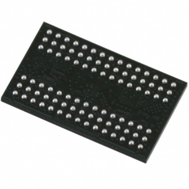
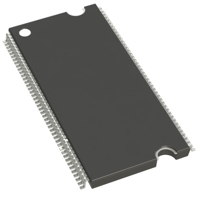
| Device Package | 90-VFBGA (8x13) | Memory Format | DRAM | Technology | SDRAM | ||
|---|---|---|---|---|---|---|---|
| Memory Size | 256 Mbit | Access Time | 6 ns | Grade | Industrial | ||
| Clock Frequency | 143 MHz | Voltage | 3V ~ 3.6V | Memory Type | Volatile | ||
| Operating Temperature | -40°C ~ 85°C (TA) | Write Cycle Time Word Page | 14 ns | Packaging | 90-VFBGA | ||
| Mounting Method | Volatile | Memory Interface | Parallel | Memory Organization | 8M x 32 | ||
| Moisture Sensitivity Level | 2 (1 Year) | RoHS Compliance | N/A | REACH Compliance | REACH Unaffected | ||
| Qualification | N/A | ECCN | EAR99 | HTS Code | 8542.32.0024 |
Overview of MT48LC8M32B2F5-7 IT – IC DRAM 256MBIT PAR 90VFBGA
The MT48LC8M32B2F5-7 IT is a 256 Mbit (8M × 32) synchronous DRAM (SDRAM) device in a 90-ball VFBGA package. It provides a parallel memory interface with internal pipelined operation and multiple on-chip features for burst access and refresh management.
Designed for systems requiring a +3.3 V supply and industrial temperature operation (−40 °C to +85 °C), this device targets applications that need deterministic SDRAM timing (143 MHz clock / 6 ns access time, speed grade -7) with programmable burst lengths and CAS latency options.
Key Features
- Memory Organization and Capacity — 8M × 32 organization (2 Meg × 32 × 4 banks) providing a total of 256 Mbit of volatile SDRAM storage.
- Core Performance — Specified for a 143 MHz clock frequency with 6 ns access time (speed grade -7); supports CAS latency settings of 1, 2 and 3.
- Burst and Access Control — Programmable burst lengths (1, 2, 4, 8, or full page) plus internal pipelined operation and internal banks to hide row access/precharge.
- Refresh and Power Modes — Auto Refresh, Self Refresh, and Auto Precharge modes; 64 ms, 4,096-cycle refresh (15.6 μs/row) supported.
- Interface and I/O — Parallel memory interface with LVTTL-compatible inputs and outputs; fully synchronous operation with signals registered on the positive edge of the system clock.
- Voltage and Timing — Single +3.3 V ±0.3 V supply (3.0 V to 3.6 V) and write cycle time (word/page) of 14 ns, providing defined timing for system integration.
- Package and Thermal — 90-ball VFBGA package (8 mm × 13 mm) with industrial operating temperature range of −40 °C to +85 °C (TA) for extended-environment designs.
Typical Applications
- PC100-compatible systems — Supports PC100 functionality for systems requiring SDRAM compliant timing and PC-class memory interfaces.
- Industrial embedded systems — Industrial temperature grade (−40 °C to +85 °C) suits controllers and embedded platforms operating in extended environments.
- Parallel SDRAM subsystems — Acts as a parallel SDRAM memory resource for designs that require 256 Mbit density, multiple banks, and programmable burst operation.
Unique Advantages
- Industrial temperature support — Rated for −40 °C to +85 °C (TA), enabling use in extended-temperature applications where thermal range is critical.
- Flexible latency and burst control — Selectable CAS latencies (1, 2, 3) and programmable burst lengths allow tuning between throughput and access granularity.
- On-chip refresh and low-management modes — Auto Refresh and Self Refresh modes reduce system refresh management overhead while maintaining data integrity.
- Compact FBGA packaging — 90-ball VFBGA (8 × 13 mm) improves board-level density for space-constrained designs.
- Standard 3.3 V supply — Operates from a single +3.3 V ±0.3 V rail (3.0–3.6 V), simplifying power supply requirements.
- Pipelined banks for reduced access stalls — Internal banks and pipelined operation help hide row access/precharge timing to maintain throughput on consecutive accesses.
Why Choose IC DRAM 256MBIT PAR 90VFBGA?
The MT48LC8M32B2F5-7 IT positions itself as a straightforward, industry-temperature SDRAM component offering 256 Mbit density with defined timing (143 MHz / 6 ns) and flexible burst/latency options. Its combination of LVTTL I/O, internal banks, and standard +3.3 V operation makes it well suited for embedded and system-memory applications that require predictable synchronous DRAM behavior.
Engineers building PC100-compatible platforms, industrial controllers, or parallel SDRAM subsystems will find this device provides a balance of capacity, timing control, and packaging density with on-chip refresh and power modes to aid system-level design and reliability.
Request a quote or submit a product inquiry for pricing and availability of the MT48LC8M32B2F5-7 IT. Include your required quantity and delivery timeframe for a faster response.