MT48LC8M32B2F5-7 TR
| Part Description |
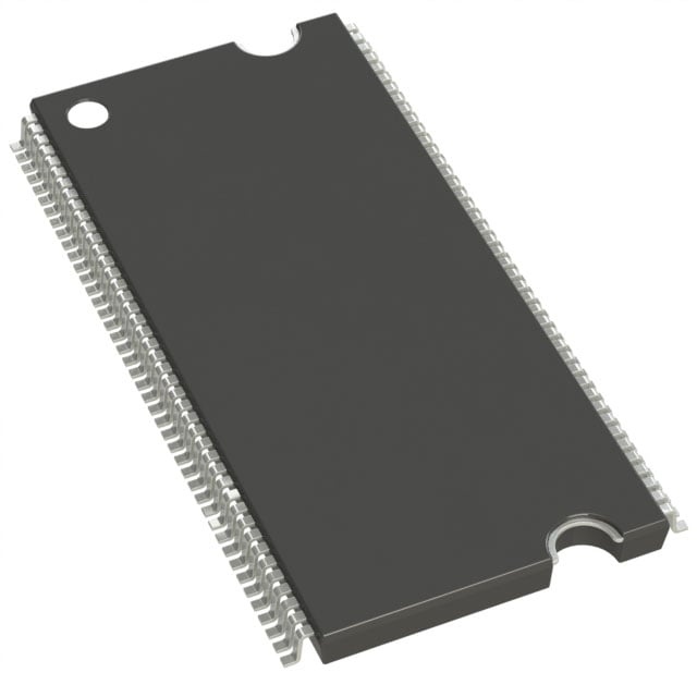
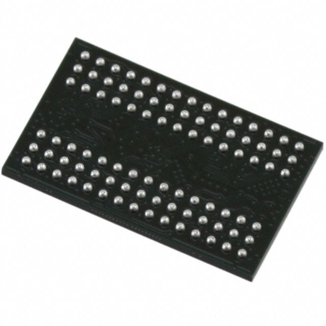
IC DRAM 256MBIT PAR 90VFBGA |
|---|---|
| Quantity | 425 Available (as of June 9, 2026) |

| Product Category | Memory |
|---|---|
| Manufacturer | Micron Technology Inc. |
| Manufacturing Status | Obsolete |
| Manufacturer Standard Lead Time | Contact Us |
| Datasheet |
Specifications & Environmental
| Device Package | 90-VFBGA (8x13) | Memory Format | DRAM | Technology | SDRAM | ||
|---|---|---|---|---|---|---|---|
| Memory Size | 256 Mbit | Access Time | 6 ns | Grade | Commercial | ||
| Clock Frequency | 143 MHz | Voltage | 3V ~ 3.6V | Memory Type | Volatile | ||
| Operating Temperature | 0°C ~ 70°C (TA) | Write Cycle Time Word Page | 14 ns | Packaging | 90-VFBGA | ||
| Mounting Method | Volatile | Memory Interface | Parallel | Memory Organization | 8M x 32 | ||
| Moisture Sensitivity Level | 2 (1 Year) | RoHS Compliance | RoHS non-compliant | REACH Compliance | REACH Unaffected | ||
| Qualification | N/A | ECCN | EAR99 | HTS Code | 8542.32.0024 |
Overview of MT48LC8M32B2F5-7 TR – IC DRAM 256MBIT PAR 90VFBGA
The MT48LC8M32B2F5-7 TR is a 256 Mbit synchronous DRAM arranged as 8M × 32 with four internal banks, supplied in a 90-ball VFBGA (8 mm × 13 mm) package. It implements fully synchronous, pipelined SDRAM functionality with a parallel memory interface suitable for commercial-temperature systems.
Designed for applications requiring a 256 Mbit parallel SDRAM solution, this device delivers PC100 functionality, programmable burst lengths, and standard SDRAM command features (auto/precharge, auto-refresh, self-refresh) while operating from a single +3.3 V ±0.3 V supply.
Key Features
- Memory Core 256 Mbit SDRAM organized as 8M × 32 with 4 internal banks (2 Meg × 32 × 4 banks) for concurrent bank operation and improved access handling.
- Synchronous, Pipelined Operation Fully synchronous design with registered inputs on the positive clock edge and internal pipelined operation that allows column addresses to change every clock cycle.
- Performance and Timing Speed grade -7 supports a clock frequency up to 143 MHz with an access time of 6.0 ns (CL = 3); supports CAS latencies of 1, 2 and 3.
- Burst and Command Flexibility Programmable burst lengths (1, 2, 4, 8, or full page) plus Auto Precharge, Concurrent Auto Precharge, Auto Refresh and Self Refresh modes.
- Interface and I/O Parallel memory interface with LVTTL-compatible inputs and outputs for standard system integration.
- Power Single +3.3 V ±0.3 V supply range (3.0 V to 3.6 V) to match common system rails.
- Package and Temperature 90-ball VFBGA package (8 mm × 13 mm footprint) with a commercial operating temperature range of 0°C to +70°C.
- Refresh and Reliability Supports a 64 ms, 4,096-cycle refresh (15.6 μs/row) and standard SDRAM refresh commands for data retention and reliability.
- Write Cycle Write cycle time (word page) specified at 14 ns for write timing planning.
Typical Applications
- Commercial embedded systems Board-level memory expansion where a 256 Mbit parallel SDRAM is required for volatile data storage in commercial-temperature designs.
- PC100-compatible systems Systems requiring PC100 functionality and standard SDRAM timing characteristics.
- Consumer electronics Devices needing parallel SDRAM buffering and burst-read/write capability with programmable burst lengths and standard SDRAM command support.
Unique Advantages
- Flexible burst operation: Programmable burst lengths (1, 2, 4, 8, full page) allow tuning of sequential transfer behavior to match system access patterns.
- Banked architecture for hidden latency: Four internal banks enable row access/precharge hiding to improve effective throughput for interleaved accesses.
- Standard 3.3 V power rail: Single +3.3 V ±0.3 V supply simplifies integration into systems with common 3.3 V rails.
- Commercial temperature rating: Specified for 0°C to +70°C operation to match typical commercial electronic applications.
- Compact FBGA footprint: 90-ball VFBGA (8 mm × 13 mm) package provides a compact board-level memory option for dense layouts.
- Synchronous LVTTL I/O: LVTTL-compatible inputs and outputs and fully synchronous operation simplify timing design and clocked interfacing.
Why Choose IC DRAM 256MBIT PAR 90VFBGA?
The MT48LC8M32B2F5-7 TR (IC DRAM 256MBIT PAR 90VFBGA) positions itself as a practical, standards-based 256 Mbit SDRAM option for commercial systems that require a parallel synchronous memory with programmable burst modes, internal bank architecture and PC100 functionality. Its combination of 8M × 32 organization, 4 banks, and standard SDRAM command set supports common memory subsystem designs.
This device is suited to engineers and procurement teams specifying board-level SDRAM for commercial embedded and legacy systems where predictable timing (6 ns access, 143 MHz clock grade), single 3.3 V supply operation, and a compact 90-ball VFBGA package are required. The product’s standard SDRAM features and documented timing make it straightforward to validate and integrate into existing memory controllers that support parallel SDRAM interfaces.
Request a quote or submit a procurement inquiry to receive pricing, lead-time and technical information for the MT48LC8M32B2F5-7 TR.