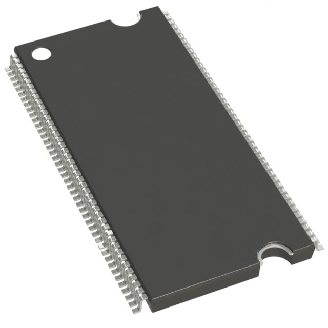
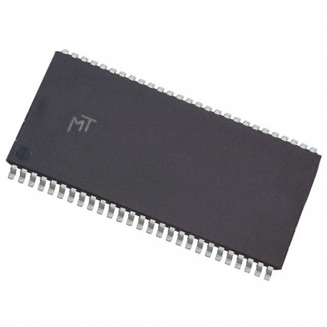
MT48LC8M32B2TG-6 TR
| Part Description |
IC DRAM 256MBIT PAR 86TSOP II |
|---|---|
| Quantity | 95 Available (as of June 15, 2026) |

| Product Category | Memory |
|---|---|
| Manufacturer | Micron Technology Inc. |
| Manufacturing Status | Obsolete |
| Manufacturer Standard Lead Time | Contact Us |
| Datasheet |
Specifications & Environmental
| Device Package | 86-TSOP II | Memory Format | DRAM | Technology | SDRAM | ||
|---|---|---|---|---|---|---|---|
| Memory Size | 256 Mbit | Access Time | 5.5 ns | Grade | Commercial | ||
| Clock Frequency | 166 MHz | Voltage | 3V ~ 3.6V | Memory Type | Volatile | ||
| Operating Temperature | 0°C ~ 70°C (TA) | Write Cycle Time Word Page | 12 ns | Packaging | 86-TFSOP (0.400", 10.16mm Width) | ||
| Mounting Method | Volatile | Memory Interface | Parallel | Memory Organization | 8M x 32 | ||
| Moisture Sensitivity Level | 2 (1 Year) | RoHS Compliance | RoHS non-compliant | REACH Compliance | REACH Unaffected | ||
| Qualification | N/A | ECCN | EAR99 | HTS Code | 8542.32.0024 |
Overview of MT48LC8M32B2TG-6 TR – IC DRAM 256MBIT PAR 86TSOP II
The MT48LC8M32B2TG-6 TR is a 256 Mbit synchronous DRAM (SDRAM) organized as 8M × 32 with four internal banks. It implements a parallel memory interface in an 86-pin TSOP II (0.400", 10.16 mm width) package and operates from a single +3.3 V ±0.3 V supply.
Designed for systems requiring standard PC100 functionality and pipelined, fully synchronous memory operation, this device delivers 166 MHz clock support with a 5.5 ns access time and programmable burst control for flexible read/write sequencing.
Key Features
- Core / Memory Architecture 8M × 32 organization (2 M × 32 × 4 banks) with internal bank architecture to hide row access and precharge latency.
- SDRAM Functionality Fully synchronous operation with internal pipelined operation, programmable burst lengths (1, 2, 4, 8, or full page), and support for Auto Precharge, Concurrent Auto Precharge and Auto Refresh modes.
- Timing & Performance -6 speed grade supports 166 MHz clock frequency and 5.5 ns access time (CAS latency options 1, 2, and 3); write cycle time (word/page) specified at 12 ns.
- Refresh & Power Modes Self Refresh mode and 4,096-cycle refresh (64 ms total) with single 3.3 V supply range (listed supply 3.0 V–3.6 V).
- I/O and Logic Levels LVTTL-compatible inputs and outputs, with all signals registered on the positive edge of the system clock.
- Package & Temperature 86-pin TSOP II (400 mil) package (10.16 mm width) for surface-mount applications; commercial operating temperature range 0 °C to +70 °C.
Typical Applications
- PC100 systems — Provides PC100 functionality for systems designed to operate with 166 MHz class SDRAM timing.
- Parallel SDRAM memory implementations — Serves as a 256 Mbit parallel SDRAM device for designs requiring an 8M × 32 memory organization and standard SDRAM command set.
- Board-level upgrades and designs — Suitable where an 86-pin TSOP II footprint and single +3.3 V supply are required.
Unique Advantages
- Standard 3.3 V supply compatibility: Operates from a single +3.3 V ±0.3 V supply (listed supply range 3.0 V–3.6 V), matching common system power rails.
- Low-latency read access: -6 speed grade provides 166 MHz clock operation with a 5.5 ns access time for responsive memory reads.
- Flexible burst control: Programmable burst lengths (1, 2, 4, 8, full page) enable tuning of transfer granularity to match system bandwidth and latency needs.
- Multi-bank architecture: Four internal banks allow overlapping row activation and precharge to improve effective throughput in pipelined systems.
- Established SDRAM command set: Supports Auto Precharge, Auto Refresh, Self Refresh and CAS latency settings (1, 2, 3) for predictable system integration.
- Compact TSOP II footprint: 86-pin TSOP (0.400", 10.16 mm) package for surface-mount assembly and board-level density.
Why Choose IC DRAM 256MBIT PAR 86TSOP II?
The MT48LC8M32B2TG-6 TR from Micron Technology, Inc. positions itself as a standard 256 Mbit SDRAM component for designs that require PC100-class timing, a parallel SDRAM interface, and a compact 86-pin TSOP II package. Its combination of 8M × 32 organization, four-bank internal architecture, and programmable burst modes provides design flexibility for pipelined and latency-sensitive memory systems.
This device is suitable for designers seeking a commercially rated SDRAM solution that aligns with 3.3 V system rails and established SDRAM command and timing conventions. Its documented timing parameters, refresh modes, and package outline support predictable integration and long-term maintainability in compatible systems.
Request a quote or submit an inquiry to receive pricing and availability details for MT48LC8M32B2TG-6 TR.