MT48LC8M32B2F5-6 TR
| Part Description |
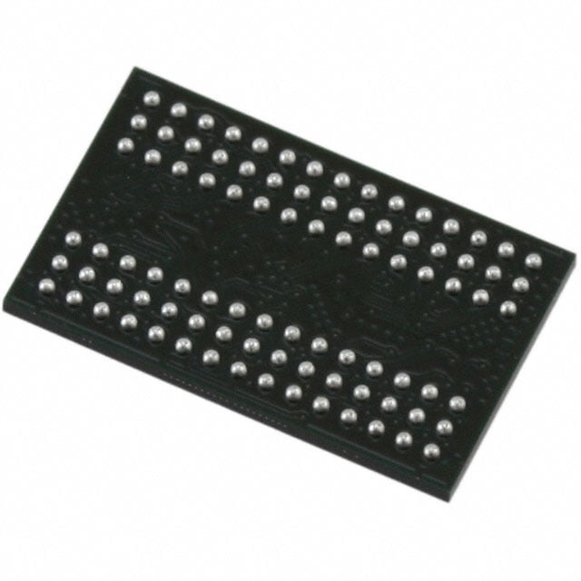
IC DRAM 256MBIT PAR 90VFBGA |
|---|---|
| Quantity | 779 Available (as of June 15, 2026) |

| Product Category | Memory |
|---|---|
| Manufacturer | Micron Technology Inc. |
| Manufacturing Status | Obsolete |
| Manufacturer Standard Lead Time | Contact Us |
| Datasheet |
Specifications & Environmental
| Device Package | 90-VFBGA (8x13) | Memory Format | DRAM | Technology | SDRAM | ||
|---|---|---|---|---|---|---|---|
| Memory Size | 256 Mbit | Access Time | 5.5 ns | Grade | Commercial | ||
| Clock Frequency | 166 MHz | Voltage | 3V ~ 3.6V | Memory Type | Volatile | ||
| Operating Temperature | 0°C ~ 70°C (TA) | Write Cycle Time Word Page | 12 ns | Packaging | 90-VFBGA | ||
| Mounting Method | Volatile | Memory Interface | Parallel | Memory Organization | 8M x 32 | ||
| Moisture Sensitivity Level | 2 (1 Year) | RoHS Compliance | RoHS non-compliant | REACH Compliance | REACH Unaffected | ||
| Qualification | N/A | ECCN | EAR99 | HTS Code | 8542.32.0024 |
Overview of MT48LC8M32B2F5-6 TR – IC DRAM 256MBIT PAR 90VFBGA
The MT48LC8M32B2F5-6 TR is a 256 Mbit ×32 synchronous DRAM (SDRAM) device from Micron Technology featuring a parallel interface and a 90-ball VFBGA package. It implements a 2M ×32 ×4-bank architecture with PC100 functionality and operates from a single +3.3 V ±0.3 V supply.
This device targets systems that require fully synchronous parallel DRAM operation at a 166 MHz clock rate (–6 speed grade) with support for programmable burst lengths, internal pipelining and bank-based row management for predictable memory access behavior.
Key Features
- Core / Organization 8M × 32 memory organization (2M ×32 ×4 banks) providing 256 Mbit total density and internal banks for row access and precharge management.
- Synchronous Operation Fully synchronous SDRAM with all signals registered on the positive edge of the system clock and internal pipelined operation allowing column address changes every clock cycle.
- Performance 166 MHz clock frequency (–6 speed grade) with an access time of 5.5 ns and write cycle time (word/page) of 12 ns.
- Burst and Latency Options Programmable burst lengths of 1, 2, 4, 8 or full page and support for CAS latency settings of 1, 2 and 3.
- Refresh and Power Management Auto Refresh and Self Refresh modes with a 64 ms, 4,096-cycle refresh (15.6 μs/row) and support for Auto Precharge and Concurrent Auto Precharge commands.
- I/O and Voltage LVTTL-compatible inputs/outputs and single +3.3 V ±0.3 V supply (operating range 3.0 V to 3.6 V specified).
- Package 90-ball VFBGA package (8 mm × 13 mm, listed as 90-VFBGA / 90-ball FBGA F5 option) suitable for compact board layouts.
- Operating Range Commercial temperature operating range: 0°C to +70°C (TA).
Typical Applications
- PC100 Memory Subsystems Designed with PC100 functionality for systems and subsystems requiring PC100-compliant synchronous DRAM behavior.
- Parallel-Interface Memory Designs Suited to designs that require a parallel SDRAM interface and predictable burst/read/write timing control.
- Space-Constrained Board Layouts The 90-ball VFBGA (8 mm × 13 mm) package supports compact PCB implementations where ball-grid packaging is preferred.
Unique Advantages
- Synchronous, pipelined architecture: Enables column address changes every clock cycle and predictable timing for pipelined memory access.
- Flexible burst and latency configuration: Programmable burst lengths and CAS latency options accommodate varied access patterns and timing requirements.
- Banked memory organization: Four internal banks help hide row access and precharge, improving effective throughput for interleaved accesses.
- Standard +3.3 V supply and LVTTL I/O: Simplifies integration with systems using industry-standard signaling and power rails.
- On-chip refresh and power modes: Auto Refresh, Self Refresh, and Auto Precharge features reduce external control complexity for refresh and power management.
- Compact FBGA package: 90-ball VFBGA (8×13 mm) reduces PCB footprint compared with larger through-hole or TSOP options.
Why Choose MT48LC8M32B2F5-6 TR?
The MT48LC8M32B2F5-6 TR provides a synchronous, banked 256 Mbit SDRAM solution with PC100 functionality and flexible burst/latency control, suited to designs that require a parallel SDRAM interface at 166 MHz. Its combination of internal pipelining, on-chip refresh modes and LVTTL I/O simplifies timing control and integration on systems powered by a +3.3 V supply.
This device is appropriate for designers and procurement teams specifying commercial-temperature SDRAM in a compact 90-ball VFBGA package where predictable synchronous performance and standard voltage/I/O compatibility are required.
Request a quote or submit an RFQ to obtain pricing and availability for the MT48LC8M32B2F5-6 TR.