MT48LC8M32B2B5-6 TR
| Part Description |
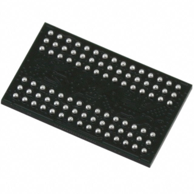
IC DRAM 256MBIT PAR 90VFBGA |
|---|---|
| Quantity | 263 Available (as of June 15, 2026) |

| Product Category | Memory |
|---|---|
| Manufacturer | Micron Technology Inc. |
| Manufacturing Status | Obsolete |
| Manufacturer Standard Lead Time | Contact Us |
| Datasheet |
Specifications & Environmental
| Device Package | 90-VFBGA (8x13) | Memory Format | DRAM | Technology | SDRAM | ||
|---|---|---|---|---|---|---|---|
| Memory Size | 256 Mbit | Access Time | 5.5 ns | Grade | Commercial | ||
| Clock Frequency | 166 MHz | Voltage | 3V ~ 3.6V | Memory Type | Volatile | ||
| Operating Temperature | 0°C ~ 70°C (TA) | Write Cycle Time Word Page | 12 ns | Packaging | 90-VFBGA | ||
| Mounting Method | Volatile | Memory Interface | Parallel | Memory Organization | 8M x 32 | ||
| Moisture Sensitivity Level | 2 (1 Year) | RoHS Compliance | ROHS3 Compliant | REACH Compliance | REACH Unaffected | ||
| Qualification | N/A | ECCN | EAR99 | HTS Code | 8542.32.0024 |
Overview of MT48LC8M32B2B5-6 TR – IC DRAM 256Mbit Parallel SDRAM (90‑VFBGA)
The MT48LC8M32B2B5-6 TR is a 256 Mbit synchronous dynamic RAM organized as 8M × 32 with four internal banks and a parallel memory interface. It provides fully synchronous, pipelined SDRAM operation with programmable burst lengths and standard SDRAM command modes.
Designed for systems requiring a 256 Mbit parallel SDRAM device in a compact ball-grid package, the device offers PC100 functionality, support for CAS latencies 1–3, and operation from a single +3.3 V supply (±0.3 V).
Key Features
- Core / Memory Organization 256 Mbit SDRAM organized as 8M × 32 (2 M × 32 × 4 banks) with internal bank architecture to hide row access and precharge operations.
- Synchronous, Pipelined Operation Fully synchronous device with all signals registered on the positive edge of the system clock and internal pipelined reads/writes; column address can be changed every clock cycle.
- Programmable Burst and Mode Support Programmable burst lengths of 1, 2, 4, 8, or full page. Supports Auto Precharge (including Concurrent Auto Precharge), Auto Refresh, and Self Refresh modes.
- Timing and Performance -6 speed grade: 6 ns cycle time (166 MHz) with 5.5 ns access time (CL = 3); write cycle (word page) time 12 ns. Supports CAS latency 1, 2, and 3.
- Power Single supply range +3.0 V to +3.6 V (single +3.3 V ±0.3 V specified in datasheet features).
- Refresh Self Refresh mode and 64 ms, 4,096-cycle refresh (15.6 µs/row) for data retention management.
- I/O Compatibility LVTTL-compatible inputs and outputs for standard logic interfacing.
- Package 90-ball VFBGA package (8 mm × 13 mm) in a 90-VFBGA (8×13) supplier device package.
- Operating Temperature Commercial temperature range: 0 °C to +70 °C (TA).
Typical Applications
- Parallel SDRAM memory subsystems Use where a 256 Mbit parallel SDRAM organized as 8M × 32 with four banks is required.
- Systems requiring PC100 functionality Designs that target PC100-compatible timing and synchronous SDRAM operation at up to 166 MHz.
Unique Advantages
- High-speed 166 MHz operation: -6 speed grade delivers a 6 ns cycle time and 5.5 ns access time (CL = 3) for timely read access.
- Flexible burst operation: Programmable burst lengths (1, 2, 4, 8, full page) simplify data transfer sequencing and maximize throughput for burst-oriented accesses.
- Internal bank architecture: Four internal banks hide row access/precharge latency, enabling pipelined commands and improved effective bandwidth.
- Standard 3.3 V supply: Single +3.3 V supply (±0.3 V) simplifies power design for systems using standard 3.3 V logic levels.
- Compact FBGA package: 90-ball VFBGA (8 × 13 mm) package supports dense board layouts while providing the required ball count for a 32-bit wide SDRAM.
- Standardized refresh and low-power modes: Auto Refresh and Self Refresh support with a 4,096-cycle refresh scheme for predictable data retention behavior.
Why Choose IC DRAM 256MBIT PAR 90VFBGA?
The MT48LC8M32B2B5-6 TR delivers a compact, parallel SDRAM solution with PC100-class timing, programmable burst operation, and a conventional 3.3 V supply. Its 8M × 32 organization with four internal banks and support for CAS latencies 1–3 provide design flexibility for systems that require synchronous, pipelined DRAM operation.
This device is suitable for designs targeting commercial temperature ranges and compact board footprints where a 90-ball VFBGA package and 256 Mbit capacity are required. The device’s standard SDRAM command set, refresh options, and LVTTL-compatible I/O support straightforward integration into parallel SDRAM memory subsystems.
Request a quote or submit a pricing and availability request to receive detailed lead times and volume pricing information for the MT48LC8M32B2B5-6 TR.