MT48LC8M32B2B5-7
| Part Description |
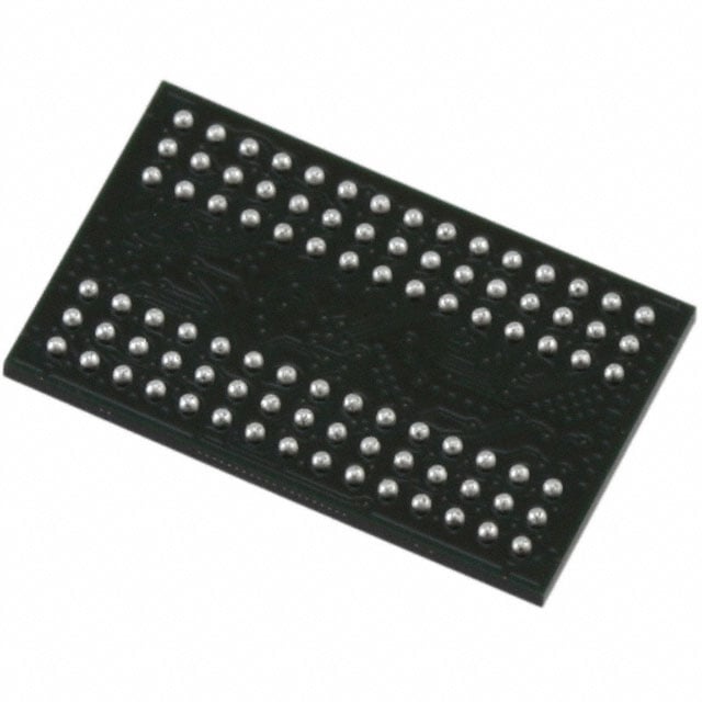
IC DRAM 256MBIT PAR 90VFBGA |
|---|---|
| Quantity | 1,360 Available (as of June 10, 2026) |

| Product Category | Memory |
|---|---|
| Manufacturer | Micron Technology Inc. |
| Manufacturing Status | Obsolete |
| Manufacturer Standard Lead Time | Contact Us |
| Datasheet |
Specifications & Environmental
| Device Package | 90-VFBGA (8x13) | Memory Format | DRAM | Technology | SDRAM | ||
|---|---|---|---|---|---|---|---|
| Memory Size | 256 Mbit | Access Time | 6 ns | Grade | Commercial | ||
| Clock Frequency | 143 MHz | Voltage | 3V ~ 3.6V | Memory Type | Volatile | ||
| Operating Temperature | 0°C ~ 70°C (TA) | Write Cycle Time Word Page | 14 ns | Packaging | 90-VFBGA | ||
| Mounting Method | Volatile | Memory Interface | Parallel | Memory Organization | 8M x 32 | ||
| Moisture Sensitivity Level | 2 (1 Year) | RoHS Compliance | ROHS Compliant | REACH Compliance | REACH Unaffected | ||
| Qualification | N/A | ECCN | EAR99 | HTS Code | 8542.32.0024 |
Overview of MT48LC8M32B2B5-7 – IC DRAM 256MBIT PAR 90VFBGA
The MT48LC8M32B2B5-7 is a 256 Mbit synchronous DRAM organized as 8M × 32 with four internal banks. It provides fully synchronous, pipelined SDRAM functionality in a 90-ball VFBGA (8 × 13 mm) package and operates from a single +3.3 V supply.
Designed for systems requiring parallel SDRAM memory with PC100-class functionality, this device offers programmable burst lengths, CAS latency options, and built-in refresh and power modes to support efficient block transfers and system-level memory management within a commercial temperature range.
Key Features
- Core / Architecture Fully synchronous SDRAM with internal pipelined operation and four internal banks (2M × 32 × 4) for improved command throughput.
- Memory Organization 256 Mbit capacity organized as 8M × 32, supporting programmable burst lengths of 1, 2, 4, 8 or full page.
- Timing & Performance –7 speed grade: 143 MHz clock frequency with 6.0 ns access time (CAS latency options 1, 2, 3) and a 14 ns write cycle time (word page).
- Refresh & Power Modes Supports Auto Refresh, Self Refresh, Concurrent Auto Precharge and a 64 ms/4,096-cycle refresh scheme (15.6 μs/row) for retained data integrity during idle periods.
- Interface & I/O Parallel memory interface with LVTTL-compatible inputs and outputs for straightforward integration with LVTTL logic domains.
- Power Single-supply operation from 3.0 V to 3.6 V (nominal +3.3 V).
- Package & Temperature 90-ball VFBGA (8 × 13 mm) supplier device package in a commercial operating temperature range of 0°C to +70°C.
- PC100 Functionality Designed to provide PC100 functionality, with synchronous signal registration on the positive clock edge and support for standard SDRAM command set.
Typical Applications
- PC100-class memory subsystems — PC100 functionality and synchronous, pipelined operation make the device suitable for systems targeting PC100 timing.
- Board-level SDRAM implementations — 256 Mbit density and 90-ball VFBGA package enable compact board-level memory configurations where parallel SDRAM is required.
- Systems requiring programmable burst transfers — Programmable burst lengths and internal banks support efficient block read/write transfers and latency hiding in parallel memory architectures.
Unique Advantages
- Flexible performance options: Multiple CAS latency settings (1, 2, 3) and programmable burst lengths allow designers to tune latency and throughput to system needs.
- Compact package footprint: 90-ball VFBGA (8 × 13 mm) package reduces board area for space-constrained designs while providing high-density memory.
- Simplified timing integration: Fully synchronous operation with signals registered on the positive clock edge and LVTTL-compatible I/O eases timing closure with standard logic domains.
- Robust refresh and power modes: Auto Refresh, Self Refresh and Concurrent Auto Precharge support background refresh and low-activity retention without external management complexity.
- Standard 3.3 V supply: Single +3.3 V ±0.3 V power supply simplifies power rail design in legacy and contemporary systems.
- Commercial temperature rating: Operates across 0°C to +70°C for applications targeting commercial ambient environments.
Why Choose MT48LC8M32B2B5-7?
The MT48LC8M32B2B5-7 combines a 256 Mbit, 8M × 32 SDRAM organization with PC100-class synchronous architecture and internal banking to deliver configurable latency and burst behavior for parallel memory designs. Its 143 MHz (–7) speed grade, LVTTL-compatible I/O, and standard +3.3 V supply make it suitable for systems that require predictable timing and compact board-level memory integration within a commercial temperature range.
This device is appropriate for designers who need a well-specified SDRAM building block offering programmable burst lengths, refresh management, and a compact 90-ball VFBGA package for dense PCB layouts. The documented timing options and power modes support predictable system behavior and long-term maintenance of stored data across idle periods.
Request a quote or submit an inquiry to obtain pricing, lead times, and availability for the MT48LC8M32B2B5-7 for your next design project.