MT48LC8M16A2TG-7E:G TR
| Part Description |
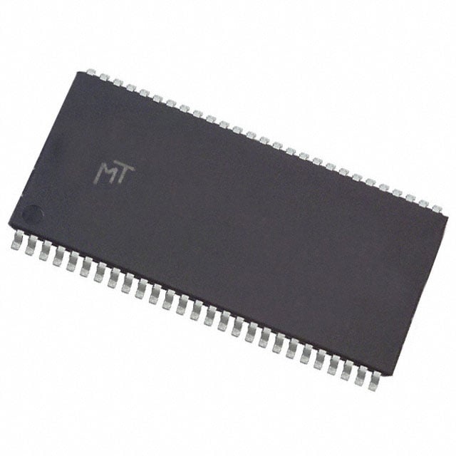
IC DRAM 128MBIT PAR 54TSOP II |
|---|---|
| Quantity | 1,616 Available (as of June 14, 2026) |
| Product Category | Memory |
|---|---|
| Manufacturer | Micron Technology Inc. |
| Manufacturing Status | Obsolete |
| Manufacturer Standard Lead Time | Contact Us |
| Datasheet |
Specifications & Environmental
| Device Package | 54-TSOP II | Memory Format | DRAM | Technology | SDRAM | ||
|---|---|---|---|---|---|---|---|
| Memory Size | 128 Mbit | Access Time | 5.4 ns | Grade | Commercial | ||
| Clock Frequency | 133 MHz | Voltage | 3V ~ 3.6V | Memory Type | Volatile | ||
| Operating Temperature | 0°C ~ 70°C (TA) | Write Cycle Time Word Page | 14 ns | Packaging | 54-TSOP (0.400", 10.16mm Width) | ||
| Mounting Method | Volatile | Memory Interface | Parallel | Memory Organization | 8M x 16 | ||
| Moisture Sensitivity Level | 3 (168 Hours) | RoHS Compliance | N/A | REACH Compliance | REACH Unaffected | ||
| Qualification | N/A | ECCN | EAR99 | HTS Code | 8542.32.0002 |
Overview of MT48LC8M16A2TG-7E:G TR – IC DRAM 128MBIT PAR 54TSOP II
The MT48LC8M16A2TG-7E:G TR is a 128 Mbit synchronous DRAM device organized as 8M × 16 with a parallel memory interface. It implements SDR SDRAM architecture with internal pipelined operation, multiple internal banks and programmable burst lengths to support synchronous system memory requirements.
Designed for systems requiring a 128 Mbit parallel SDRAM in a 54‑pin TSOP II package, the device provides PC100/PC133 timing grades, single‑supply operation at 3.3 V (±0.3 V), and standard commercial temperature operation (0 °C to +70 °C).
Key Features
- Memory Architecture — 128 Mbit capacity organized as 8M × 16 with 4 internal banks for efficient row access and precharge handling.
- SDR SDRAM Core — Fully synchronous operation with all signals registered on the positive edge of the system clock and internal pipelined operation allowing column address changes every clock cycle.
- Timing Grades and Performance — PC100 and PC133 compliant; the -7E speed grade targets 133 MHz with a 2-2-2 (RCD-RP-CL) timing profile as specified in the datasheet.
- Burst and Refresh — Programmable burst lengths (1, 2, 4, 8, full page), auto precharge modes, auto refresh and self refresh modes with 4096‑cycle refresh intervals documented in the datasheet.
- Interface and I/O — LVTTL‑compatible inputs and outputs and a parallel memory interface suitable for synchronous memory subsystems.
- Power — Single 3.3 V ±0.3 V supply (3.0 V to 3.6 V) for standard commercial systems.
- Package and Temperature — 54‑pin TSOP II (400 mil, 10.16 mm width) plastic package; commercial operating temperature range 0 °C to +70 °C.
Typical Applications
- Synchronous memory subsystems — Acts as a parallel SDRAM component in systems that require PC100/PC133 synchronous DRAM devices for buffering and working memory.
- Embedded systems with parallel DRAM — Suitable where a 128 Mbit parallel SDRAM in a 54‑pin TSOP II package is required for system memory or frame buffering.
- Legacy or board‑level designs — Fits designs that employ parallel SDRAM interfaces and need a 3.3 V, commercial‑temperature memory device.
Unique Advantages
- Synchronous, pipelined operation: Registered inputs on the positive clock edge and internal pipelining permit predictable timing and the ability to change column addresses each cycle.
- Flexible burst and refresh options: Programmable burst lengths plus auto precharge, auto refresh and self‑refresh modes simplify controller design and refresh management.
- PC100/PC133 compatibility: Timing grades documented for PC100 and PC133 enable integration into systems targeting these clock domains.
- Compact TSOP II packaging: 54‑pin TSOP II (400 mil) provides a slim, board‑mountable footprint for designs constrained by PCB area.
- Standard 3.3 V supply: Single 3.3 V ±0.3 V operation aligns with common system power rails for easy integration.
Why Choose IC DRAM 128MBIT PAR 54TSOP II?
The MT48LC8M16A2TG-7E:G TR positions itself as a straightforward 128 Mbit SDRAM option for designers needing a parallel, synchronous memory device in a 54‑pin TSOP II footprint. With PC100/PC133 timing options, internal bank architecture and a range of programmable burst and refresh modes, it supports deterministic memory behavior in commercial-temperature systems running from a standard 3.3 V supply.
Choose this device for designs that require a documented SDRAM timing profile, LVTTL-compatible I/O and a compact package for board-level integration. The device’s documented features and timing grades make it suitable for systems and customers building or maintaining parallel SDRAM memory subsystems.
Request a quote or submit an inquiry to obtain pricing and availability information for the MT48LC8M16A2TG-7E:G TR.