MT48LC8M32B2B5-7 IT TR
| Part Description |
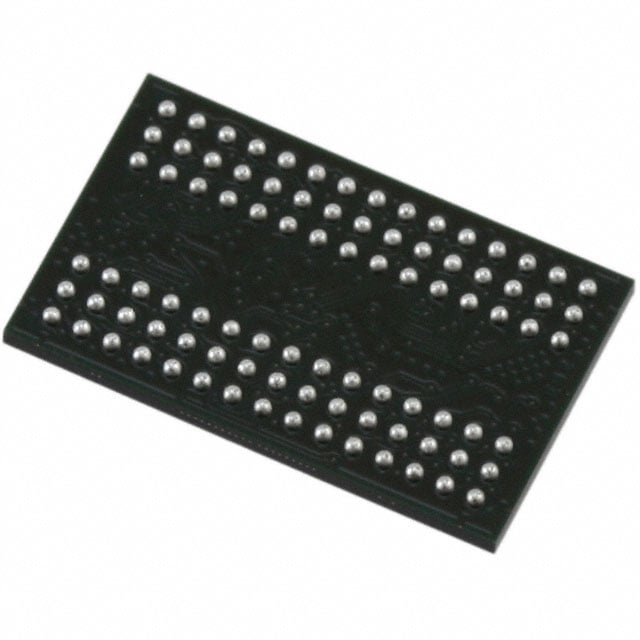
IC DRAM 256MBIT PAR 90VFBGA |
|---|---|
| Quantity | 563 Available (as of June 9, 2026) |

| Product Category | Memory |
|---|---|
| Manufacturer | Micron Technology Inc. |
| Manufacturing Status | Obsolete |
| Manufacturer Standard Lead Time | Contact Us |
| Datasheet |
Specifications & Environmental
| Device Package | 90-VFBGA (8x13) | Memory Format | DRAM | Technology | SDRAM | ||
|---|---|---|---|---|---|---|---|
| Memory Size | 256 Mbit | Access Time | 6 ns | Grade | Industrial | ||
| Clock Frequency | 143 MHz | Voltage | 3V ~ 3.6V | Memory Type | Volatile | ||
| Operating Temperature | -40°C ~ 85°C (TA) | Write Cycle Time Word Page | 14 ns | Packaging | 90-VFBGA | ||
| Mounting Method | Volatile | Memory Interface | Parallel | Memory Organization | 8M x 32 | ||
| Moisture Sensitivity Level | 2 (1 Year) | RoHS Compliance | ROHS Compliant | REACH Compliance | REACH Unaffected | ||
| Qualification | N/A | ECCN | EAR99 | HTS Code | 8542.32.0024 |
Overview of MT48LC8M32B2B5-7 IT TR – IC DRAM 256Mbit Parallel 90‑VFBGA
The MT48LC8M32B2B5-7 IT TR is a 256Mbit synchronous DRAM organized as 8M × 32 with 4 internal banks. It implements fully synchronous operation with LVTTL-compatible I/O and a parallel memory interface to support system memory applications requiring pipelined, burst-capable DRAM.
Designed for industrial-temperature operation (−40°C to +85°C), this device supports a 3.3V ±0.3V supply and a −7 speed grade (143 MHz / 6.0 ns access time), offering programmable burst lengths, auto-refresh/self-refresh modes and compact 90‑ball VFBGA packaging (8 mm × 13 mm).
Key Features
- Core / Architecture 8M × 32 organization with 4 internal banks for bank-management and hidden row access, enabling internal pipelined operation and column address changes every clock cycle.
- Memory Type & Capacity 256 Mbit SDRAM (DRAM) in a parallel interface format, supporting burst lengths of 1, 2, 4, 8 or full-page operation.
- Performance & Timing −7 speed grade: 143 MHz clock frequency and 6.0 ns access time (CAS latency options 1, 2, 3). Write cycle time (word/page) specified at 14 ns.
- Power Single supply operation at +3.3V ±0.3V.
- Refresh & Power Modes Auto Refresh, Concurrent Auto Precharge, and Self Refresh Mode with 4,096-cycle refresh (64 ms) supported to maintain data integrity.
- Interface & Compatibility Fully synchronous operation with LVTTL‑compatible inputs/outputs and PC100 functionality.
- Package 90‑ball VFBGA package (8 mm × 13 mm / 90‑VFBGA) for board-level density in compact layouts.
- Temperature Range Industrial grade operation: −40°C to +85°C (TA) — available on the −7 speed grade.
Typical Applications
- PC100-compliant memory subsystems — Use in systems that require PC100 functionality and synchronous DRAM with burst capabilities.
- Embedded systems with parallel SDRAM interfaces — Board-level memory expansion where a parallel SDRAM interface and pipelined access are required.
- Industrial equipment — Systems operating across −40°C to +85°C that need a 256Mbit SDRAM in a compact FBGA package.
Unique Advantages
- Flexible Burst Operation: Programmable burst lengths (1, 2, 4, 8, full page) enable tuning for sequential and random access patterns.
- Banked Architecture for Throughput: Four internal banks and internal pipelining allow column addresses to change every clock cycle, improving sustained access efficiency.
- Industrial Temperature Support: Rated for −40°C to +85°C, providing suitability for temperature-challenging environments on the −7 grade.
- Compact FBGA Package: 90‑ball VFBGA (8×13 mm) delivers high density with a small board footprint for space-constrained designs.
- Comprehensive Refresh & Low-Power Modes: Auto Refresh and Self Refresh modes with 4,096-cycle/64 ms refresh scheme help manage data retention and power.
- Standard 3.3V Supply: Single +3.3V ±0.3V supply simplifies power-rail design in systems using legacy 3.3V logic levels.
Why Choose MT48LC8M32B2B5-7 IT TR?
The MT48LC8M32B2B5-7 IT TR combines a standard, fully synchronous SDRAM architecture with industrial-grade temperature range and a compact 90‑ball FBGA package, making it suitable for embedded and system memory applications that require pipelined, burst-capable parallel DRAM. With PC100 functionality, selectable CAS latencies, and internal bank management, it provides deterministic timing and flexible access modes for designers targeting 3.3V systems.
This device is appropriate for designers needing a verified 256Mbit x32 DRAM solution with refresh management and low-power modes, backed by Micron's documented DRAM specifications and timing parameters for system integration and validation.
Request a quote or submit a pricing and availability inquiry for MT48LC8M32B2B5-7 IT TR to receive lead-time and volume pricing information.