MT53E512M64D4NW-053 WT:E TR
| Part Description |
IC DRAM 32GBIT 1.866GHZ 432VFBGA |
|---|---|
| Quantity | 300 Available (as of June 15, 2026) |

| Product Category | Memory |
|---|---|
| Manufacturer | Micron Technology Inc. |
| Manufacturing Status | Obsolete |
| Manufacturer Standard Lead Time | Contact Us |
| Datasheet |
Specifications & Environmental
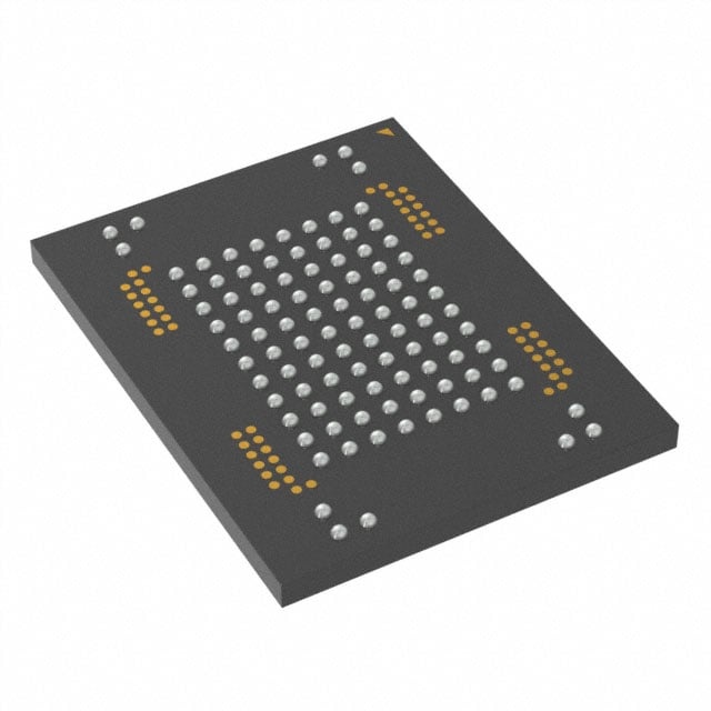
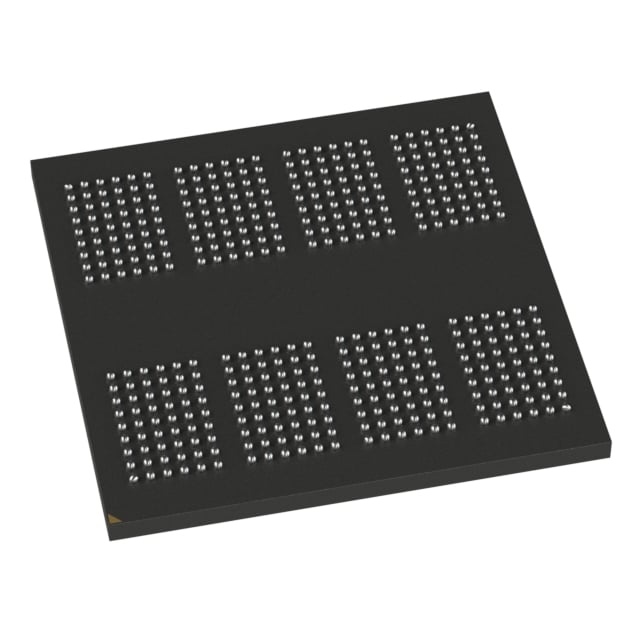
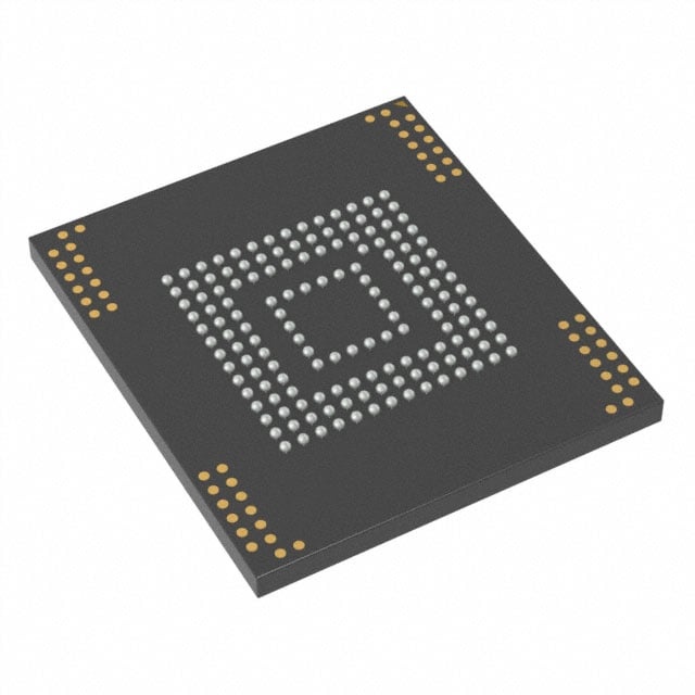
| Device Package | 432-VFBGA (15x15) | Memory Format | DRAM | Technology | SDRAM - Mobile LPDDR4 | ||
|---|---|---|---|---|---|---|---|
| Memory Size | 32 Gbit | Access Time | N/A | Grade | Industrial | ||
| Clock Frequency | 1.866 GHz | Voltage | 1.1V | Memory Type | Volatile | ||
| Operating Temperature | -30°C ~ 85°C (TC) | Write Cycle Time Word Page | N/A | Packaging | 432-VFBGA | ||
| Mounting Method | Volatile | Memory Interface | N/A | Memory Organization | 512M x 64 | ||
| Moisture Sensitivity Level | N/A | RoHS Compliance | Unknown | REACH Compliance | REACH Unknown | ||
| Qualification | N/A | ECCN | OBSOLETE | HTS Code | 0000.00.0000 |
Overview of MT53E512M64D4NW-053 WT:E TR – IC DRAM 32GBIT 1.866GHZ 432VFBGA
The MT53E512M64D4NW-053 WT:E TR is a 32 Gbit volatile DRAM device implemented as Mobile LPDDR4 SDRAM in a 432-ball VFBGA (15×15) package. It is organized as 512M x 64 and specified with a clock frequency of 1.866 GHz and a 1.1 V supply.
Designed for compact systems requiring high-density, low-voltage dynamic memory, this LPDDR4-family device offers programmable latencies and burst lengths, multiple internal banks for concurrent operation, and on-die power and thermal management features documented in the Micron LPDDR4X/LPDDR4 datasheet.
Key Features
- Core / Memory Architecture Mobile LPDDR4 SDRAM organized as 512M × 64 delivering 32 Gbit of DRAM capacity in a multi-die package configuration described by Micron.
- Performance Clock frequency of 1.866 GHz (data rate per pin as specified by the device family) with 16n prefetch DDR architecture and up to eight internal banks for concurrent operation and improved command scheduling.
- Programmable Timing and Burst Supports programmable READ and WRITE latencies (RL/WL) and selectable on-the-fly burst lengths (BL = 16, 32) for flexible timing optimization.
- Power and Voltage Ultra-low-voltage operation with a nominal 1.10 V supply; datasheet family notes configurable core and I/O power supplies and selectable termination (programmable VSS, ODT).
- Reliability / Thermal Management On-chip temperature sensor and partial-array self refresh (PASR) support for adaptive self-refresh control and thermal-aware operation.
- System Features Directed per-bank refresh for concurrent bank operation, selectable output drive strength (DS), and clock-stop capability to aid power-managed designs.
- Package & Mechanical 432-VFBGA package (15×15 mm) optimized for space-constrained boards; operating temperature range of −30°C to +85°C (TC) is specified for this ordering option (WT).
- Standards & Compliance The device family documentation indicates RoHS-compliant, “green” packaging as part of the LPDDR4X/LPDDR4 product description.
Typical Applications
- Mobile and Handheld Devices Low-voltage LPDDR4 memory suited to compact, battery-powered designs that require high-density DRAM in a small package.
- Embedded Memory Subsystems Acts as high-density volatile memory for SoC-connected memory channels where programmable latencies and burst lengths enable timing tuning.
- High-Bandwidth Subsystems Supports applications that leverage multiple internal banks and high data rates for sustained bandwidth in graphics or streaming data paths.
Unique Advantages
- High-density in a compact package: 32 Gbit capacity in a 432-VFBGA (15×15) package enables high memory capacity while conserving PCB area.
- Low-voltage operation: Nominal 1.10 V supply reduces core/I/O power requirements compared with higher-voltage DRAM options within the LPDDR4 family.
- Flexible timing and burst control: Programmable READ/WRITE latencies and burst lengths (BL = 16, 32) allow designers to optimize performance and latency for targeted workloads.
- Bank-level refresh and thermal control: Directed per-bank refresh and an on-chip temperature sensor support concurrent operation and adaptive self-refresh strategies.
- Power-management features: Selectable output drive strength, clock-stop capability, and programmable termination options aid in system-level power tuning.
Why Choose MT53E512M64D4NW-053 WT:E TR?
The MT53E512M64D4NW-053 WT:E TR positions itself as a compact, low-voltage LPDDR4 DRAM solution for designs that require high density, configurable timing, and on-die thermal and power management features. Its 512M × 64 organization and 432-ball VFBGA package deliver an integration-friendly option where board space and power efficiency are important.
This device is suited to engineers building mobile and embedded systems that need predictable, datasheet-defined LPDDR4 capabilities—programmable latencies, burst control, directed per-bank refresh, and on-chip monitoring—backed by Micron’s LPDDR4X/LPDDR4 product documentation.
Request a quote or submit an inquiry for MT53E512M64D4NW-053 WT:E TR to receive pricing and availability details from our sales team.