MT53E512M64D4NW-046 IT:E TR
| Part Description |
IC DRAM 32GBIT 2.133GHZ 432VFBGA |
|---|---|
| Quantity | 1,548 Available (as of June 14, 2026) |

| Product Category | Memory |
|---|---|
| Manufacturer | Micron Technology Inc. |
| Manufacturing Status | Obsolete |
| Manufacturer Standard Lead Time | Contact Us |
| Datasheet |
Specifications & Environmental
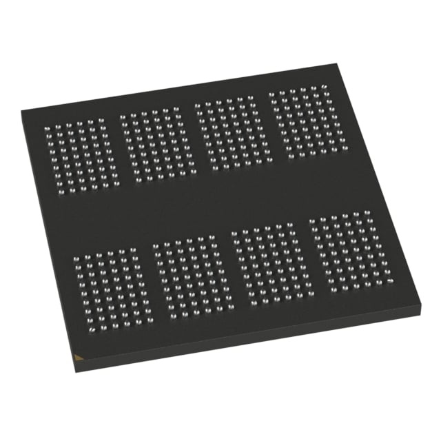
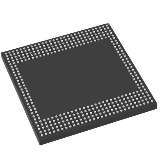
| Device Package | 432-VFBGA (15x15) | Memory Format | DRAM | Technology | SDRAM - Mobile LPDDR4 | ||
|---|---|---|---|---|---|---|---|
| Memory Size | 32 Gbit | Access Time | N/A | Grade | Automotive | ||
| Clock Frequency | 2.133 GHz | Voltage | 1.1V | Memory Type | Volatile | ||
| Operating Temperature | -40°C ~ 95°C (TC) | Write Cycle Time Word Page | N/A | Packaging | 432-VFBGA | ||
| Mounting Method | Volatile | Memory Interface | N/A | Memory Organization | 512M x 64 | ||
| Moisture Sensitivity Level | 3 (168 Hours) | RoHS Compliance | ROHS3 Compliant | REACH Compliance | REACH Unknown | ||
| Qualification | N/A | ECCN | OBSOLETE | HTS Code | N/A |
Overview of MT53E512M64D4NW-046 IT:E TR – IC DRAM 32 Gbit 2.133 GHz 432-VFBGA
The MT53E512M64D4NW-046 IT:E TR is a 32 Gbit volatile DRAM device implemented in Mobile LPDDR4/LPDDR4X SDRAM technology. It provides a 512M x 64 memory organization, a 2.133 GHz clock rate (4266 Mb/s data rate per pin) and is offered in a 432-ball Very Fine Ball Grid Array (15 × 15 mm) package.
Targeted at systems requiring high data throughput and low-voltage operation, this device combines LPDDR4/LPDDR4X architecture, programmable timing and low-voltage supplies to support high-bandwidth memory subsystems within temperature ranges down to –40°C and up to 95°C.
Key Features
- Architecture & Performance — LPDDR4/LPDDR4X SDRAM with 16n prefetch DDR architecture, 8 internal banks per channel, and a data rate of 4266 Mb/s per pin (clock rate 2133 MHz).
- Memory Organization & Capacity — 32 Gbit total density configured as 512M × 64 to support wide data paths and large memory footprints.
- Speed Grade & Timing — Speed grade -046 (2133 MHz) with documented READ and WRITE latency options (e.g., RL/WL sets and DBI-enabled latencies up to RL=36/40 as shown for the -046 grade).
- Low-Voltage Power Options — Ultra-low-voltage supplies with nominal VDD2/VDDQ = 1.10 V (datasheet lists VDD1 = 1.70–1.95 V, VDD2 = 1.06–1.17 V, and VDDQ options 0.57–0.65 V or 1.06–1.17 V).
- Power and Refresh Features — Directed per-bank refresh for concurrent bank operation, partial-array self refresh (PASR), on-chip temperature sensor to control self-refresh behavior, and clock-stop capability.
- Programmability and I/O — Programmable READ/WRITE latencies (RL/WL), selectable output drive strength (DS), programmable VSS (ODT) termination, and bidirectional/differential data strobe per byte lane.
- Package and Thermal — 432-VFBGA (15 × 15 mm) package; specified operating temperature range –40°C to +95°C (TC).
- Throughput per Die — Datasheet specifies up to 8.5 GB/s per die for a x16 channel configuration.
- Compliance — Datasheet indicates RoHS-compliant, “green” packaging.
Typical Applications
- Mobile and Handheld Devices — Low-voltage LPDDR4/LPDDR4X memory suited to mobile designs that need high data rates within constrained power budgets.
- Embedded High-Bandwidth Memory Subsystems — Wide 64-bit organization and high per-pin data rates support embedded systems that require sustained throughput.
- Thermally Demanding Environments — Extended operating range (–40°C to +95°C) allows use in systems with broad temperature requirements.
Unique Advantages
- High per-pin data rate: 4266 Mb/s per pin (2133 MHz clock) enables high-bandwidth memory channels tied directly to documented speed-grade timing.
- Low-voltage operation: Nominal VDD2/VDDQ of 1.10 V and ultra-low-voltage core/I/O options reduce supply requirements compared to higher-voltage DRAM.
- Flexible timing and drive control: Programmable RL/WL, selectable output drive strength, and programmable ODT allow tuning for system timing and signal integrity.
- Concurrent refresh and power management: Directed per-bank refresh and on-chip temperature sensing support concurrent operation and adaptive self-refresh management.
- Compact package: 432-ball VFBGA (15 × 15 mm) provides a high-density, space-efficient footprint for board-level integration.
- Extended temperature support: –40°C to +95°C rating addresses applications requiring wide thermal range operation.
Why Choose MT53E512M64D4NW-046 IT:E TR?
This Micron LPDDR4/LPDDR4X device positions itself as a high-bandwidth, low-voltage DRAM option with programmable timing, per-bank refresh capabilities, and an extended operating temperature range. Its 32 Gbit density in a 512M × 64 organization and 432-VFBGA footprint make it suitable for designs that need wide memory buses and compact packaging.
Designers seeking documented speed-grade performance (4266 Mb/s per pin, -046 timing), flexible power options, and features that support concurrent refresh and thermal-aware self-refresh will find this device applicable for embedded and mobile memory subsystems where throughput, voltage scalability, and thermal range are key considerations.
Request a quote or submit an inquiry to sales for pricing, lead-time and availability information for the MT53E512M64D4NW-046 IT:E TR.