MT53E512M64D4NK-046 WT:D TR
| Part Description |
IC DRAM 32GBIT 2.133GHZ 366WFBGA |
|---|---|
| Quantity | 126 Available (as of June 10, 2026) |

| Product Category | Memory |
|---|---|
| Manufacturer | Micron Technology Inc. |
| Manufacturing Status | Obsolete |
| Manufacturer Standard Lead Time | Contact Us |
| Datasheet |
Specifications & Environmental
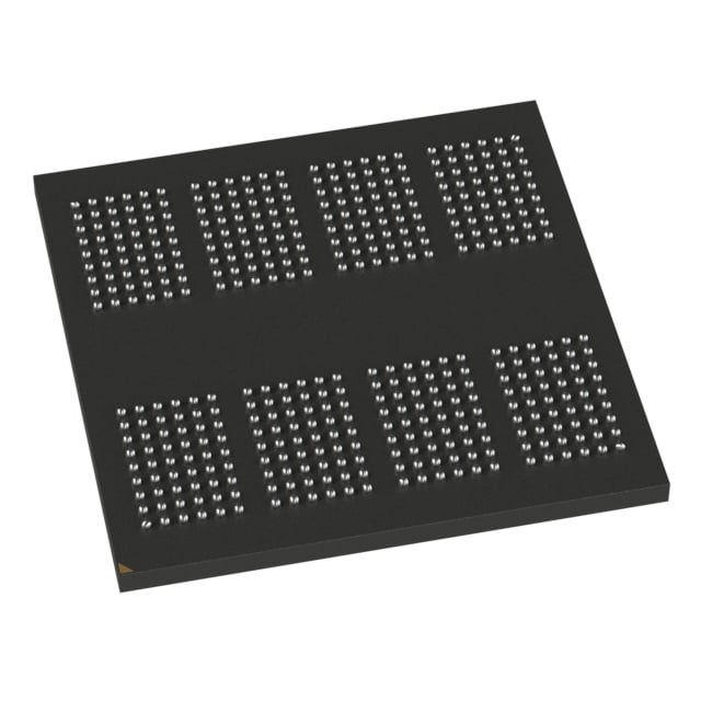
| Device Package | 366-WFBGA (15x15) | Memory Format | DRAM | Technology | SDRAM - Mobile LPDDR4 | ||
|---|---|---|---|---|---|---|---|
| Memory Size | 32 Gbit | Access Time | N/A | Grade | Industrial | ||
| Clock Frequency | 2.133 GHz | Voltage | 1.1V | Memory Type | Volatile | ||
| Operating Temperature | -30°C ~ 85°C (TC) | Write Cycle Time Word Page | N/A | Packaging | 366-WFBGA | ||
| Mounting Method | Volatile | Memory Interface | N/A | Memory Organization | 512M x 64 | ||
| Moisture Sensitivity Level | 3 (168 Hours) | RoHS Compliance | ROHS3 Compliant | REACH Compliance | REACH Unaffected | ||
| Qualification | N/A | ECCN | OBSOLETE | HTS Code | 0000.00.0000 |
Overview of MT53E512M64D4NK-046 WT:D TR – IC DRAM 32GBIT 2.133GHZ 366WFBGA
The MT53E512M64D4NK-046 WT:D TR is a 32 Gbit volatile DRAM device implemented in mobile LPDDR4/LPDDR4X SDRAM architecture. It delivers high-rate mobile memory performance in a compact 366-ball WFBGA package (15×15 mm), targeting mobile and portable system memory applications.
Designed for high-bandwidth embedded memory use, the device offers 2.133 GHz clock operation (4266 Mb/s data rate per pin), low-voltage operation, and features that support concurrent bank operation and programmable timing to match system requirements.
Key Features
- Memory Architecture 32 Gbit density organized as 512M × 64 with 16n prefetch DDR architecture and 8 internal banks per channel for concurrent operation.
- High Data Rate Clock frequency 2.133 GHz with a data rate per pin of 4266 Mb/s (speed grade -046) suitable for bandwidth-intensive mobile memory subsystems.
- Low-Voltage Operation Product nominal supply shown as 1.1V; datasheet lists core and I/O supply options including VDD1 = 1.70–1.95V (1.80V nominal), VDD2 = 1.06–1.17V (1.10V nominal), and VDDQ options of 0.57–0.65V (0.60V nominal) or 1.06–1.17V (1.10V nominal).
- Programmable Timing and Burst Control Supports programmable READ/WRITE latencies (RL/WL) and programmable on-the-fly burst lengths (BL = 16, 32) to adapt throughput and latency to system needs.
- Refresh and Power Management Directed per-bank refresh enables concurrent bank operation and easier command scheduling; on-chip temperature sensor and partial-array self refresh (PASR) support adaptive self-refresh control.
- Signal and Drive Options Bidirectional/differential data strobe per byte lane, selectable output drive strength (DS), programmable VSS (ODT) termination, and clock-stop capability.
- Package and Temperature 366-WFBGA (15×15 mm) package; operating temperature range specified as −30°C to +85°C (TC).
- Performance per Channel Datasheet notes up to 8.5 GB/s per die ×16 channel performance capability for high-throughput configurations.
Typical Applications
- Mobile and Portable Devices Memory for mobile LPDDR4/LPDDR4X-based designs requiring compact, low-voltage, high-data-rate DRAM.
- Embedded Memory Subsystems High-density embedded DRAM for systems that require concurrent bank operation and programmable timing.
- Bandwidth-Intensive Features Applications that benefit from elevated per-channel throughput where 4266 Mb/s per pin and multi-bank concurrency are needed.
Unique Advantages
- High-density, compact package: 32 Gbit capacity in a 366-ball WFBGA (15×15 mm) package minimizes board area for dense system layouts.
- High data-rate capability: 2.133 GHz clock and 4266 Mb/s per-pin data rate support demanding memory bandwidth requirements.
- Flexible power options: Low-voltage operation and multiple VDD options in the datasheet enable power-optimized system designs.
- Concurrent-bank operation: Directed per-bank refresh and 8 internal banks per channel improve command scheduling and effective concurrency.
- Programmability for tuning: Configurable RL/WL and burst length (BL = 16, 32) allow designers to tune latency and throughput trade-offs.
- Temperature-aware power control: On-chip temperature sensing and PASR help optimize self-refresh behavior across operating conditions.
Why Choose MT53E512M64D4NK-046 WT:D TR?
This Micron LPDDR4/LPDDR4X device combines high-density 32 Gbit memory organization with 2.133 GHz clock operation in a space-efficient 366-WFBGA package. Its low-voltage modes, programmable timing options, and banked architecture make it suitable for designs that require configurable performance and efficient power management.
The device is appropriate for embedded and mobile applications where bandwidth, density, and compact packaging are primary considerations, and where on-die features such as temperature sensing and partial-array self refresh aid system-level power and thermal management.
Request a quote or submit a pricing inquiry to receive availability and lead-time information for MT53E512M64D4NK-046 WT:D TR.