MT53E512M64D4NK-053 WT:D
| Part Description |
IC DRAM 32GBIT 1.866GHZ 366WFBGA |
|---|---|
| Quantity | 579 Available (as of June 15, 2026) |
| Product Category | DRAM Memory |
|---|---|
| Manufacturer | Micron Technology Inc. |
| Manufacturing Status | Obsolete |
| Manufacturer Standard Lead Time | Contact Us |
| Datasheet |
Specifications & Environmental
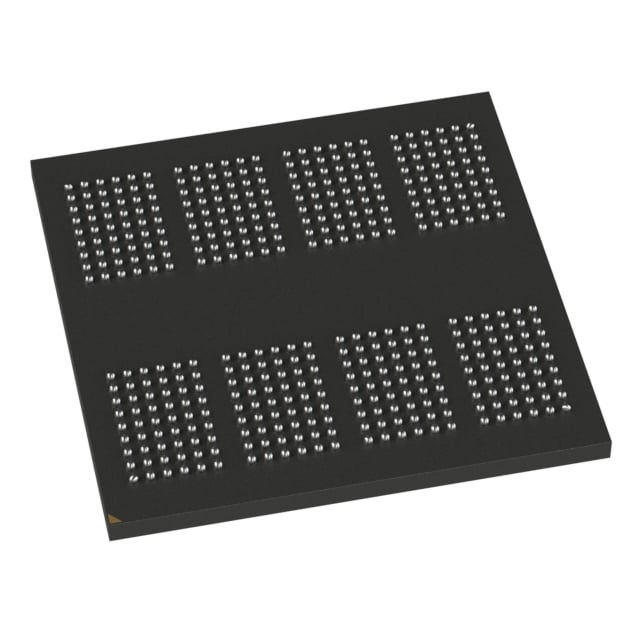
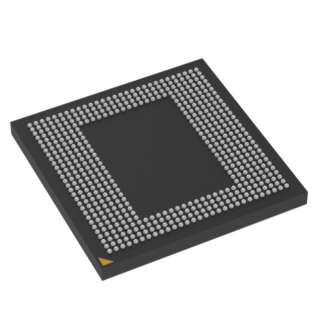
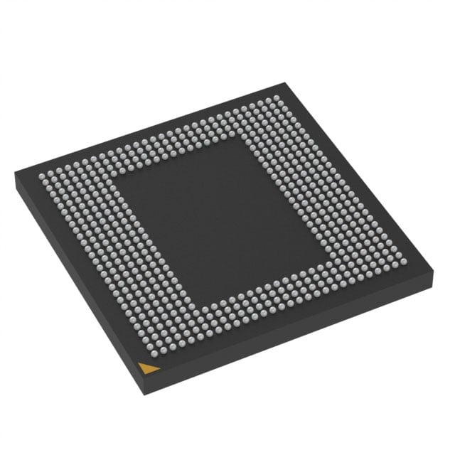
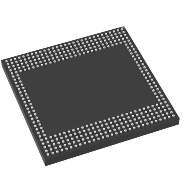
| Device Package | 366-WFBGA (15x15) | Memory Format | DRAM | Technology | SDRAM - Mobile LPDDR4 | ||
|---|---|---|---|---|---|---|---|
| Memory Size | 32 Gbit | Access Time | N/A | Grade | Industrial | ||
| Clock Frequency | 1.866 GHz | Voltage | 1.1V | Memory Type | Volatile | ||
| Operating Temperature | -30°C ~ 85°C (TC) | Write Cycle Time Word Page | N/A | Packaging | 366-WFBGA | ||
| Mounting Method | Volatile | Memory Interface | N/A | Memory Organization | 512M x 64 | ||
| Moisture Sensitivity Level | 3 (168 Hours) | RoHS Compliance | ROHS3 Compliant | REACH Compliance | REACH Unaffected | ||
| Qualification | N/A | ECCN | OBSOLETE | HTS Code | 0000.00.0000 |
Overview of MT53E512M64D4NK-053 WT:D – IC DRAM 32GBIT 1.866GHZ 366WFBGA
The MT53E512M64D4NK-053 WT:D is a 32 Gbit volatile DRAM device implemented in Mobile LPDDR4 SDRAM technology with a 512M × 64 organization. It delivers a 1.866 GHz clock frequency in a 366-ball WFBGA (15 × 15 mm) package and targets designs that require high-density, low-voltage mobile DRAM.
Designed for compact, power-conscious systems, this device pairs ultra-low-voltage core and I/O supplies with LPDDR4/LPDDR4X feature sets to support high-bandwidth memory operation in space-constrained packages across an operating range of −30°C to +85°C (TC).
Key Features
- Core Architecture LPDDR4/LPDDR4X SDRAM family characteristics including 16n prefetch DDR architecture and programmable READ/WRITE latencies for flexible timing control.
- Density & Organization 32 Gbit total capacity organized as 512M × 64, enabling high-density memory integration in a single package.
- Performance 1.866 GHz clock rate (data rate per pin and speed grade options provided in the datasheet) for high-throughput memory operation.
- Low-Voltage Operation Ultra-low-voltage core and I/O supplies. Datasheet nominal values include VDD1 ≈ 1.80 V and VDD2 ≈ 1.10 V; VDDQ options include 0.60 V or 1.10 V variants.
- Power Management & Low-Power Modes On-chip temperature sensor, partial-array self refresh (PASR), directed per-bank refresh, and clock-stop capability to optimize power and refresh behavior.
- Data Integrity & Timing Bidirectional/differential data strobe per byte lane, selectable output drive strength, programmable on-die termination (VSS ODT), and support for BL = 16 or 32 burst lengths.
- Package & Thermal 366-WFBGA (15 × 15 mm) package for compact board-level integration and an operating temperature range of −30°C to +85°C (TC).
Typical Applications
- Mobile devices High-density, low-voltage memory for compact mobile and handheld systems where package footprint and power are constrained.
- Embedded computing Local DRAM for system-on-module and embedded platforms requiring 32 Gbit capacity and LPDDR4 performance characteristics.
- Memory modules and multi-die packages Integration into high-density memory configurations using the 366-WFBGA package and LPDDR4 timing features.
Unique Advantages
- High density in a compact package: 32 Gbit capacity (512M × 64) in a 15 × 15 mm 366-WFBGA package reduces PCB area for high-capacity designs.
- Low-voltage operation: Ultra-low-voltage core/I/O with VDD2 ≈ 1.10 V support lowers system power budget for battery-powered applications.
- Flexible timing and burst options: Programmable READ/WRITE latencies and selectable burst lengths (BL = 16, 32) allow designers to tune performance to workload requirements.
- Power and refresh controls: Directed per-bank refresh, PASR, and on-chip temperature monitoring enable efficient refresh scheduling and reduced power during idle periods.
- Integration-ready I/O: Differential/bidirectional data strobes per byte lane and programmable drive strength simplify interface timing and signal integrity tuning.
Why Choose IC DRAM 32GBIT 1.866GHZ 366WFBGA?
This MT53E512M64D4NK-053 WT:D device positions itself as a high-density LPDDR4 memory building block that combines compact packaging, low-voltage operation, and configurable performance parameters. It is well suited for designers requiring substantial on-package memory capacity with LPDDR4 feature support and power-management options.
Ideal for mobile and embedded systems that demand reduced footprint and controlled power consumption, the device offers scalable timing and refresh features to match diverse system requirements while operating across a wide temperature range.
Request a quote or submit an inquiry to discuss availability, lead times, and integration support for the MT53E512M64D4NK-053 WT:D.