MT53E512M64D4HJ-046 WT:D TR
| Part Description |
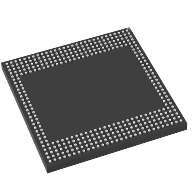
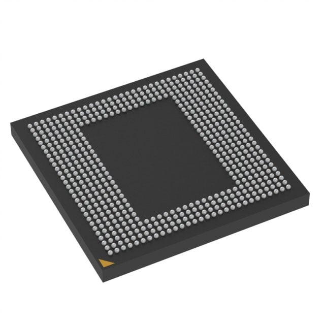
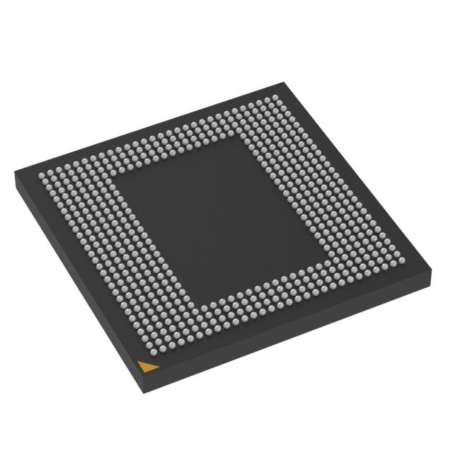
IC DRAM 32GBIT PAR 556WFBGA |
|---|---|
| Quantity | 731 Available (as of June 15, 2026) |
| Product Category | Memory |
|---|---|
| Manufacturer | Micron Technology Inc. |
| Manufacturing Status | Obsolete |
| Manufacturer Standard Lead Time | Contact Us |
| Datasheet |
Specifications & Environmental
| Device Package | N/A | Memory Format | DRAM | Technology | SDRAM - Mobile LPDDR4 | ||
|---|---|---|---|---|---|---|---|
| Memory Size | 32 Gbit | Access Time | N/A | Grade | N/A | ||
| Clock Frequency | N/A | Voltage | N/A | Memory Type | N/A | ||
| Operating Temperature | N/A | Write Cycle Time Word Page | N/A | Packaging | N/A | ||
| Mounting Method | N/A | Memory Interface | Parallel | Memory Organization | 512M x 64 | ||
| Moisture Sensitivity Level | N/A | RoHS Compliance | Unknown | REACH Compliance | REACH Unknown | ||
| Qualification | N/A | ECCN | OBSOLETE | HTS Code | N/A |
Overview of MT53E512M64D4HJ-046 WT:D TR – IC DRAM 32GBIT PAR 556WFBGA
The MT53E512M64D4HJ-046 WT:D TR is a 32 Gbit LPDDR4 SDRAM device organized as 512M x 64 with a parallel memory interface. It is offered in a 556-ball package and follows the LPDDR4/LPDDR4X unified product specification described in the datasheet.
Targeted at mobile LPDDR4 applications, this device supports high per-pin data rates (4266 Mb/s at the -046 speed grade), programmable latencies and burst lengths, and features aimed at efficient, concurrent memory operation.
Key Features
- Core / Architecture 16n prefetch DDR architecture with 8 internal banks per channel for concurrent operation; array configured as 512M × 64 (4 channels × 16 I/O).
- Performance -046 speed grade: 2133 MHz clock rate (4266 Mb/s data rate per pin); up to 8.5 GB/s per die ×16 channel reported in the datasheet.
- Power Ultra-low-voltage core and I/O supplies. Documented supply ranges include VDD1 = 1.70–1.95 V, VDD2 = 1.06–1.17 V, and VDDQ = 0.57–0.65 V (0.60 V nominal) or 1.06–1.17 V (1.10 V nominal) in LPDDR4X/LPDDR4 mode.
- Latency and Burst Control Programmable READ and WRITE latencies (RL/WL) and selectable burst lengths (BL = 16, 32) for flexible timing and throughput tuning.
- Refresh and Reliability Directed per-bank refresh for concurrent bank operation, partial-array self refresh (PASR), on‑chip temperature sensor for self-refresh control, and programmable VSS (ODT) termination.
- Interface and Signals Single-data-rate CMD/ADR entry, bidirectional/differential data strobe per byte lane, and support for single-ended CK and DQS.
- Package and Temperature 556-ball TFBGA package (12.4 mm × 12.4 mm × 1.1 mm, Ø0.24 SMD) — HJ option; operating temperature range for the WT option: –25°C to +85°C. RoHS-compliant packaging noted in the datasheet.
Typical Applications
- Mobile devices and handhelds LPDDR4 architecture and mobile voltage options make this device suitable for memory subsystems in mobile-class designs.
- High-bandwidth embedded systems High per-pin data rates and programmable latencies support designs requiring sustained memory throughput.
- Memory expansion for LPDDR4 SoCs 512M × 64 organization and parallel interface support integration with LPDDR4-compatible memory controllers for expanded system memory.
Unique Advantages
- High per-pin data rate: 4266 Mb/s (2133 MHz clock, -046 speed grade) enables elevated throughput for data-intensive operations.
- Low-voltage operation: Multiple VDD options including ultra-low VDDQ values reduce power draw where supported by system design.
- Flexible timing control: Programmable RL/WL and selectable burst lengths (BL = 16, 32) allow tuning for specific performance/latency trade-offs.
- Concurrent bank operation: Directed per-bank refresh and 8 internal banks per channel improve scheduling flexibility and effective bandwidth.
- Compact BGA footprint: 556-ball TFBGA (12.4 mm × 12.4 mm) offers a high-density package option for space-constrained assemblies.
- Thermal and self-refresh features: On-chip temperature sensor and partial-array self refresh help manage retention and power in variable thermal conditions.
Why Choose MT53E512M64D4HJ-046 WT:D TR?
This Micron LPDDR4X/LPDDR4 device provides a combination of high data rate capability, low-voltage operation, and configurable timing that is aligned with mobile LPDDR4 system requirements. Its 512M × 64 organization and 32 Gbit capacity deliver a practical balance of density and parallel I/O for designs that demand scalable memory bandwidth.
Engineers designing mobile-class and high-bandwidth embedded systems will find value in the device’s programmable latencies, directed refresh capabilities, and compact 556-ball TFBGA package. The documented electrical and timing options support integration into LPDDR4-based memory subsystems where those specific parameters are required.
Request a quote or contact sales to discuss availability, ordering quantities, and application-specific requirements for MT53E512M64D4HJ-046 WT:D TR.