W25N512GVBIG
| Part Description |
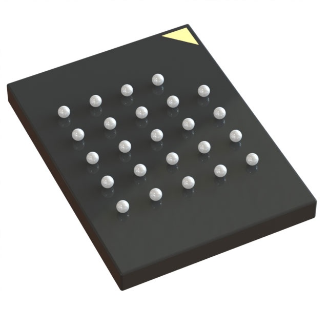
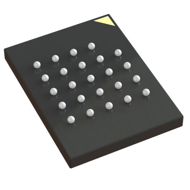
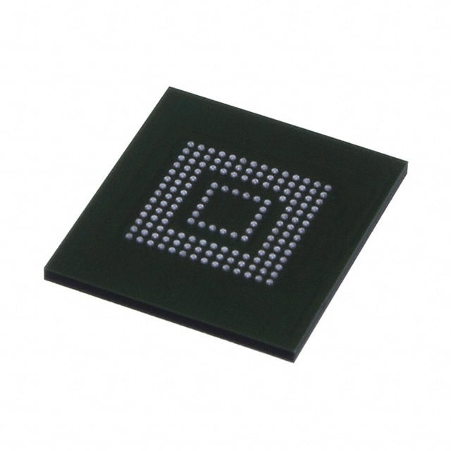
IC FLASH 512MBIT SPI 24TFBGA |
|---|---|
| Quantity | 196 Available (as of June 14, 2026) |

| Product Category | Memory |
|---|---|
| Manufacturer | Winbond Electronics |
| Manufacturing Status | Active |
| Manufacturer Standard Lead Time | 28 Weeks |
| Datasheet |
Specifications & Environmental
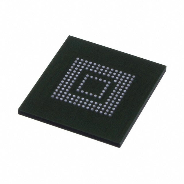
| Device Package | 24-TFBGA (6x8) | Memory Format | FLASH | Technology | FLASH - NAND (SLC) | ||
|---|---|---|---|---|---|---|---|
| Memory Size | 512 Mbit | Access Time | 7 ns | Grade | Industrial | ||
| Clock Frequency | 166 MHz | Voltage | 2.7V ~ 3.6V | Memory Type | Non-Volatile | ||
| Operating Temperature | -40°C ~ 85°C (TA) | Write Cycle Time Word Page | 700 μs | Packaging | 24-TBGA | ||
| Mounting Method | Non-Volatile | Memory Interface | SPI - Quad I/O | Memory Organization | 64M x 8 | ||
| Moisture Sensitivity Level | 3 (168 Hours) | RoHS Compliance | ROHS3 Compliant | REACH Compliance | REACH Unaffected | ||
| Qualification | N/A | ECCN | 3A991B1A | HTS Code | 8542.32.0071 |
Overview of W25N512GVBIG – IC FLASH 512MBIT SPI 24TFBGA
The W25N512GVBIG is a 3.0V, 512 Mbit serial SLC NAND Flash memory device with Dual/Quad SPI support and buffer/continuous read modes. It provides non-volatile storage in a compact 24-TFBGA (6×8 mm) package for embedded and storage-focused applications.
Designed for serial flash storage, the device targets systems requiring organized 64M × 8 memory, flexible SPI interfaces, and operation across a -40°C to 85°C ambient range, with a supply voltage window of 2.7V to 3.6V.
Key Features
- Memory Type & Technology 512 Mbit non-volatile SLC NAND flash organized as 64M × 8 for reliable single-level cell storage.
- Serial SPI Interface Supports Standard, Dual and Quad SPI modes (Quad I/O) for flexible serial connectivity.
- High-Speed Clock Operates with a clock frequency up to 166 MHz to support fast serial read operations.
- Read/Buffer Modes Buffer Read and Continuous Read modes are supported for efficient data transfer and sustained read throughput.
- Program/Erase & Bad Block Management Includes program execute, 128KB block erase and bad block management features as documented in device instruction set.
- Protection & Configuration Protection, configuration and status registers with OTP-lockable bits and an ECC enable bit for configurable device protection and error reporting.
- Performance Characteristics Typical access time cited as 7 ns and a write (word/page) cycle time of 700 µs for programming operations.
- Power Supply Single-supply operation from 2.7V to 3.6V, specified as a 3V device in the datasheet.
- Package & Temperature Supplied in a 24-TFBGA (6×8 mm) package and specified for operation from -40°C to 85°C (TA).
Typical Applications
- Embedded Firmware Storage Non-volatile SLC NAND storage for boot code and firmware images requiring organized 64M × 8 memory.
- Serial Data Storage External serial flash for system data and lookup tables, using Dual/Quad SPI for higher throughput.
- Industrial Control Systems Use in equipment that benefits from the device’s -40°C to 85°C operating range and compact TFBGA package.
- Consumer and IoT Devices Code and data storage in space-constrained designs that require a 3V serial NAND flash solution.
Unique Advantages
- Serial SLC NAND Architecture: Provides single-level cell flash organization (64M × 8) for non-volatile data retention and predictable storage layout.
- Flexible SPI Modes: Dual and Quad SPI plus buffer/continuous read modes give designers options to balance pin usage and sustained read performance up to a 166 MHz clock.
- Integrated Protection and ECC Controls: Protection, configuration and status registers with OTP-lockable bits and an ECC enable option enable configurable data integrity and device locking.
- Industrial Temperature Range: Specified operation from -40°C to 85°C supports deployments in temperature-challenging environments.
- Wide Supply Range: 2.7V to 3.6V supply tolerance allows compatibility with common 3V system rails.
- Compact BGA Package: 24-TFBGA (6×8 mm) package offers a small footprint for space-constrained PCB designs.
Why Choose W25N512GVBIG?
The W25N512GVBIG combines 512 Mbit SLC NAND storage, Dual/Quad SPI connectivity and buffer/continuous read modes in a compact 24-TFBGA package, offering a practical balance of capacity, interface flexibility and thermal range for embedded and general-purpose serial storage needs. Its register-based protection, ECC enable option and documented instruction set (including block erase and bad block management) support robust integration into firmware and data-storage workflows.
This device is well suited for designers seeking a 3V, SPI-accessible NAND flash with organized memory (64M × 8), clear programming and protection controls, and operation across industrial temperature conditions.
Request a quote or submit an inquiry to receive pricing, availability and lead-time information for the W25N512GVBIG.