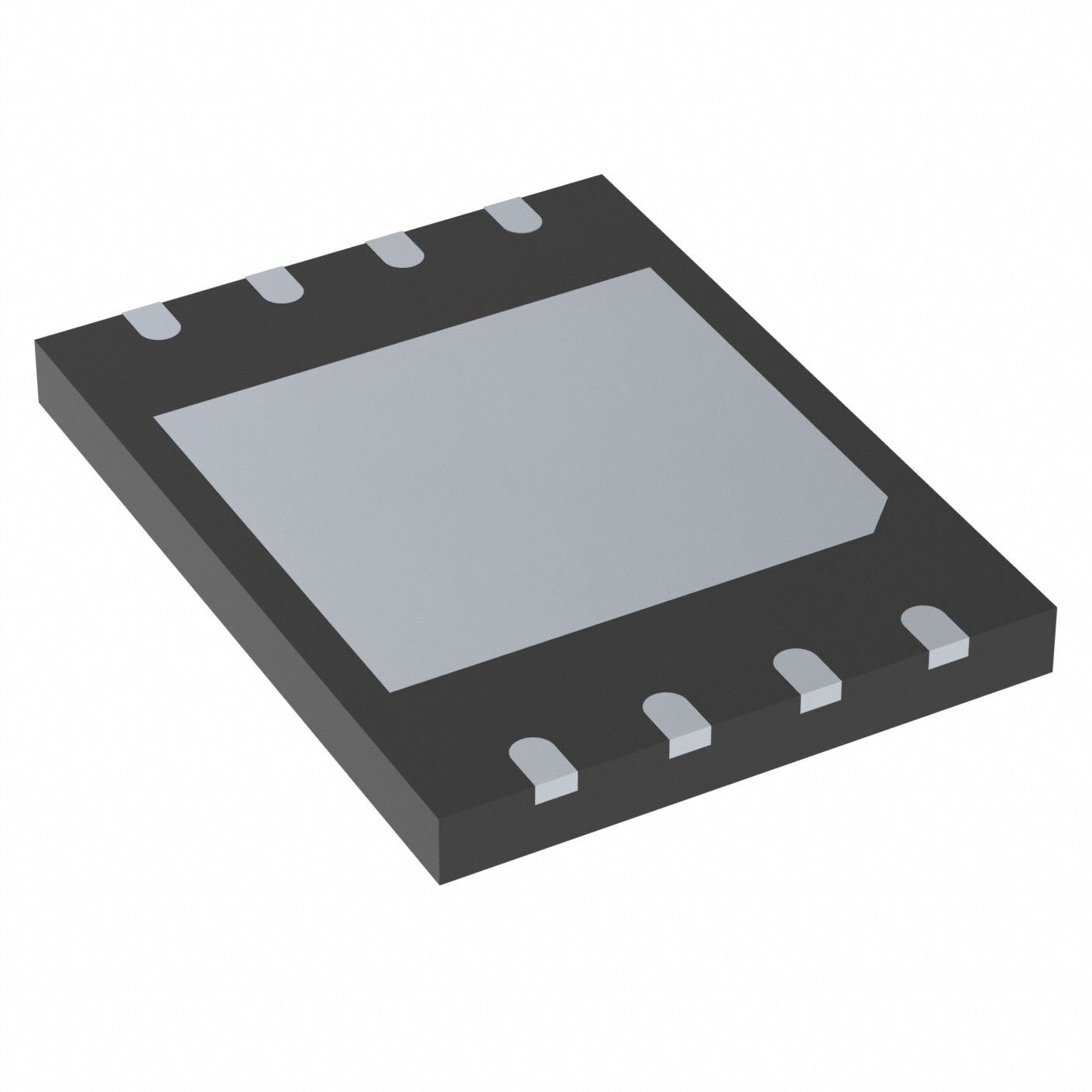
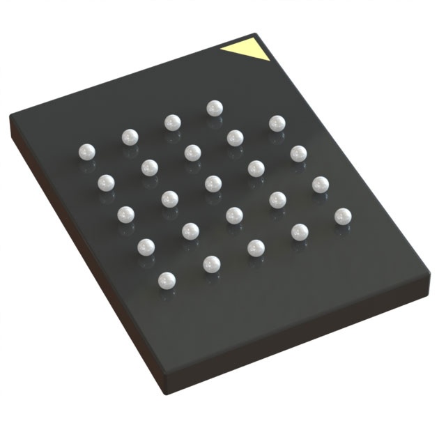
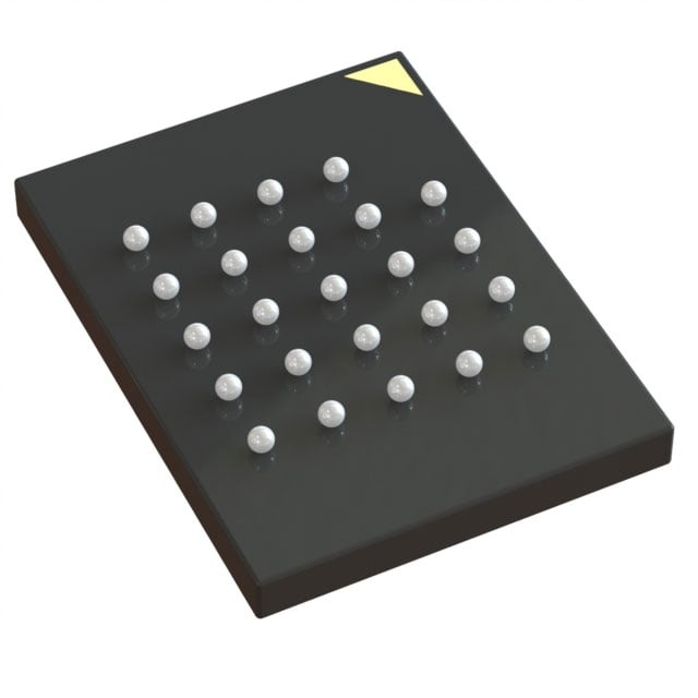
W25N512GVBIT
| Part Description |
IC FLASH 512MBIT SPI 24TFBGA |
|---|---|
| Quantity | 1,751 Available (as of June 9, 2026) |
| Product Category | Memory |
|---|---|
| Manufacturer | Winbond Electronics |
| Manufacturing Status | Active |
| Manufacturer Standard Lead Time | 28 Weeks |
| Datasheet |
Specifications & Environmental
| Device Package | 24-TFBGA (6x8) | Memory Format | FLASH | Technology | FLASH - NAND (SLC) | ||
|---|---|---|---|---|---|---|---|
| Memory Size | 512 Mbit | Access Time | 7 ns | Grade | Industrial | ||
| Clock Frequency | 166 MHz | Voltage | 2.7V ~ 3.6V | Memory Type | Non-Volatile | ||
| Operating Temperature | -40°C ~ 85°C (TA) | Write Cycle Time Word Page | 700 μs | Packaging | 24-TBGA | ||
| Mounting Method | Non-Volatile | Memory Interface | SPI - Quad I/O | Memory Organization | 64M x 8 | ||
| Moisture Sensitivity Level | 3 (168 Hours) | RoHS Compliance | ROHS3 Compliant | REACH Compliance | REACH Unaffected | ||
| Qualification | N/A | ECCN | 3A991B1A | HTS Code | 8542.32.0071 |
Overview of W25N512GVBIT – IC FLASH 512MBIT SPI 24TFBGA
The W25N512GVBIT is a 3V, 512 M-bit serial SLC NAND flash memory device from Winbond's SpiFlash® family. It provides serial Dual/Quad SPI interface with buffer read and continuous read modes and is organized as 64M × 8 bits in a 24-TFBGA (6×8 mm) package.
Designed for non-volatile storage in embedded designs, the device offers clock operation up to 166 MHz, an access time of 7 ns, and a supply voltage range of 2.7 V to 3.6 V. On-chip protection, ECC status reporting and bad block management features support reliable block and page operations.
Key Features
- Memory Architecture
512 Mbit SLC NAND flash organized as 64M × 8 for byte-wide access and large on-board storage capacity. - Serial Interface
SPI interface with Dual and Quad I/O support for flexible signaling modes and command sets. - Read Modes
Buffer read and continuous read modes are supported to optimize sequential data access patterns. - Performance
Supports clock operation up to 166 MHz with an access time of 7 ns for low-latency read transactions. - Program/Erase
128 KB block erase support and program execute commands; typical word/page write cycle time specified at 700 µs. - Protection and Management
Includes protection/configuration/status registers (volatile and OTP-lockable options), bad block management, BBM look-up support, and status registers reporting ECC and program/erase failure flags. - Voltage and Temperature
Supply voltage range 2.7 V to 3.6 V; operating temperature range −40 °C to 85 °C (TA). - Package
24-TFBGA (6×8 mm) supplier device package providing a compact BGA footprint.
Typical Applications
- Embedded Systems
Non-volatile serial flash storage for embedded devices requiring SLC NAND memory with Dual/Quad SPI access. - Firmware and Boot Storage
Storage of firmware and boot code using continuous and buffer read modes for sequential code retrieval. - Block Storage and Data Logging
Large-block erase (128 KB) and bad block management support storage of log or large data blocks with on-chip management features.
Unique Advantages
- Large SLC Capacity: 512 Mbit organized as 64M × 8 provides substantial non-volatile storage in a single device.
- Flexible SPI I/O Modes: Dual and Quad SPI support plus buffer/continuous read modes let designers select I/O and read strategies that match system requirements.
- Defined Performance Parameters: 166 MHz clock frequency and 7 ns access time provide clear, measurable timing characteristics for system integration.
- On‑Chip Management: Bad block management, BBM lookup, ECC status reporting and configurable protection registers help maintain data integrity and control memory access.
- Wide Voltage and Temperature Range: 2.7 V–3.6 V supply and −40 °C to 85 °C operating range accommodate a variety of embedded operating environments.
- Compact BGA Package: 24-TFBGA (6×8 mm) package minimizes board footprint while providing a reliable solder-down mounting option.
Why Choose W25N512GVBIT?
The W25N512GVBIT positions itself as a 3V serial SLC NAND flash device offering substantial storage capacity with Dual/Quad SPI access, structured protection registers, and on-chip memory management features such as bad block handling and ECC status reporting. Its documented timing (166 MHz clock, 7 ns access) and defined program/erase behavior (128 KB block erase, 700 µs write cycle time) make integration and performance budgeting straightforward for hardware and firmware teams.
This device is suited to designs that need a compact, high-capacity serial flash solution in a 24-TFBGA package and require explicit configuration and status controls for reliable non-volatile storage across a −40 °C to 85 °C operating range.
Request a quote or contact sales for pricing, lead-time and additional technical information about the W25N512GVBIT.