W25N512GWPIR
| Part Description |
IC FLASH 512MBIT SPI/QUAD 8WSON |
|---|---|
| Quantity | 611 Available (as of June 14, 2026) |
| Product Category | Memory |
|---|---|
| Manufacturer | Winbond Electronics |
| Manufacturing Status | Active |
| Manufacturer Standard Lead Time | 24 Weeks |
| Datasheet |
Specifications & Environmental
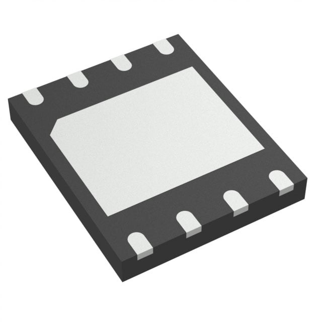
| Device Package | 8-WSON (6x5) | Memory Format | FLASH | Technology | FLASH - NAND (SLC) | ||
|---|---|---|---|---|---|---|---|
| Memory Size | 512 Mbit | Access Time | 7 ns | Grade | Industrial | ||
| Clock Frequency | 104 MHz | Voltage | 1.7V ~ 1.95V | Memory Type | Non-Volatile | ||
| Operating Temperature | -40°C ~ 85°C (TA) | Write Cycle Time Word Page | 700 μs | Packaging | 8-WDFN Exposed Pad | ||
| Mounting Method | Non-Volatile | Memory Interface | SPI - Quad I/O | Memory Organization | 64M x 8 | ||
| Moisture Sensitivity Level | 3 (168 Hours) | RoHS Compliance | ROHS3 Compliant | REACH Compliance | REACH Unaffected | ||
| Qualification | N/A | ECCN | 3A991B1A | HTS Code | 8542.32.0071 |
Overview of W25N512GWPIR – IC FLASH 512MBIT SPI/QUAD 8WSON
The W25N512GWPIR from Winbond Electronics is a 1.8V, 512 M-bit serial SLC NAND flash memory in the SpiFlash® family, offering Dual and Quad SPI interfaces. It implements buffer read and continuous read modes and provides non-volatile storage with a 64M x 8 memory organization.
Designed for systems requiring high-density serial flash with configurable SPI modes, the device combines high-speed serial access (up to 104 MHz clock) and on-device protection/configuration registers to support controlled program/erase operations and data integrity features from the datasheet.
Key Features
- Memory Type and Capacity Non-volatile SLC NAND flash with a total memory size of 512 Mbit organized as 64M x 8.
- Interface Options Supports Standard SPI, Dual SPI and Quad SPI (Quad I/O) for flexible serial connectivity.
- Read Modes Buffer Read and Continuous Read modes are supported to optimize sequential data access.
- Performance Up to 104 MHz serial clock frequency and a listed access time of 7 ns for fast read responsiveness.
- Program/Erase Characteristics Specifies a write cycle time (word/page) of 700 µs and includes instructions for block erase and program execute operations in the instruction set.
- Protection and Status Registers Volatile-writable protection and configuration registers (including block protect bits, write-protect enable, OTP lockable bits and ECC enable) plus multiple status registers for device state and error reporting.
- Bad Block Management & ECC Includes bad block management instructions and cumulative ECC status reporting as part of the status register architecture.
- Supply Voltage Operates from 1.7 V to 1.95 V to match low-voltage system rails.
- Package Available in an 8-WSON (6 × 5 mm) package with exposed pad (8-WDFN), suitable for compact board designs.
- Operating Temperature Rated for ambient operation from −40°C to 85°C (TA).
Unique Advantages
- High-density serial storage: 512 Mbit SLC NAND provides significant non-volatile capacity in a small serial package for embedded memory expansion.
- Flexible high-speed SPI access: Dual/Quad SPI support and up to 104 MHz clock enables faster serial throughput compared to single-line SPI modes.
- Optimized sequential reads: Buffer Read and Continuous Read modes reduce overhead for long transfers and simplify streaming access patterns.
- On-device protection and ECC controls: Protection/configuration registers and ECC enable bits provide software-accessible controls for block protection, OTP locking and error reporting.
- Low-voltage operation: 1.7 V to 1.95 V supply range supports integration into low-voltage platforms and simplifies power-rail requirements.
- Compact package footprint: 8-WSON (6×5 mm) with exposed pad delivers a space-efficient form factor for board-level integration.
Why Choose W25N512GWPIR?
The W25N512GWPIR positions itself as a compact, high-density serial SLC NAND flash solution with flexible Dual/Quad SPI interfaces and dedicated read modes for efficient sequential access. Its documented protection registers, ECC status reporting and bad block management functions address common flash management needs while the 1.7 V–1.95 V supply range and −40°C to 85°C operating window support a broad set of embedded system conditions defined in the product data.
This device is suited to designs that require sizable non-volatile storage in a small package with configurable SPI performance and explicit on-device controls for programming, erase and status monitoring as described in the datasheet.
If you need pricing, lead times or a formal quote for W25N512GWPIR, request a quote or submit an inquiry for sales and availability details.