W25N512GWPIT
| Part Description |
IC FLASH 512MBIT SPI/QUAD 8WSON |
|---|---|
| Quantity | 826 Available (as of June 10, 2026) |

| Product Category | Memory |
|---|---|
| Manufacturer | Winbond Electronics |
| Manufacturing Status | Active |
| Manufacturer Standard Lead Time | 24 Weeks |
| Datasheet |
Specifications & Environmental
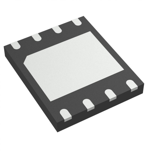
| Device Package | 8-WSON (6x5) | Memory Format | FLASH | Technology | FLASH - NAND (SLC) | ||
|---|---|---|---|---|---|---|---|
| Memory Size | 512 Mbit | Access Time | 7 ns | Grade | Industrial | ||
| Clock Frequency | 104 MHz | Voltage | 1.7V ~ 1.95V | Memory Type | Non-Volatile | ||
| Operating Temperature | -40°C ~ 85°C (TA) | Write Cycle Time Word Page | 700 μs | Packaging | 8-WDFN Exposed Pad | ||
| Mounting Method | Non-Volatile | Memory Interface | SPI - Quad I/O | Memory Organization | 64M x 8 | ||
| Moisture Sensitivity Level | 3 (168 Hours) | RoHS Compliance | ROHS3 Compliant | REACH Compliance | REACH Unaffected | ||
| Qualification | N/A | ECCN | 3A991B1A | HTS Code | 8542.32.0071 |
Overview of W25N512GWPIT – IC FLASH 512MBIT SPI/QUAD 8WSON
The W25N512GWPIT is a 512 M-bit serial SLC NAND flash memory offering Dual/Quad SPI operation with buffer read and continuous read modes. It implements a 64M x 8 memory organization and is designed for non-volatile serial storage in systems using SPI/Quad I/O interfaces.
Key architectural attributes include 1.8V-class operation (1.7 V to 1.95 V supply range), a Quad/Dual SPI interface up to a 104 MHz clock, and a compact 8-WSON (6 × 5 mm) package with exposed pad. The device provides on-chip protection and status/configuration registers for program/erase management and ECC control.
Key Features
- Memory — 512 Mbit SLC NAND flash organized as 64M × 8 for serial non-volatile storage.
- Interface — SPI with Dual and Quad I/O support enabling higher I/O throughput and compatibility with standard serial flash interfaces.
- Performance — Supports clock frequencies up to 104 MHz and documented access time of 7 ns; includes buffer read and continuous read modes for efficient data transfer.
- Power — Low-voltage operation with supply range from 1.7 V to 1.95 V (1.8V-class).
- Program/Erase and Timing — Write cycle time (word/page program) specified at 700 µs and dedicated instructions for program execute and block erase operations.
- Protection & Status — Multiple protection and configuration registers (volatile and OTP-lockable bits), write protection, and status registers including ECC status and program/erase failure indicators.
- Bad Block Management — On-chip bad block management and lookup table functions exposed via instruction set.
- Operating Range — Specified for operation from −40 °C to 85 °C (TA).
- Package — Supplied in an 8-WDFN/8-WSON (6 × 5 mm) package with exposed pad for compact board integration.
Typical Applications
- Embedded Non-volatile Storage — Provides 512 M-bit SLC NAND flash for systems that require serial flash storage accessible over SPI/Quad I/O.
- Firmware and Code Storage — Stores boot images, firmware or application code with support for program execute and dedicated read modes.
- Data Logging and Parameter Storage — Non-volatile storage for logged data and configuration parameters with bad block management and status reporting.
Unique Advantages
- 1.8V-class Operation: Designed for 1.7 V to 1.95 V systems for direct compatibility with 1.8 V designs.
- Quad/Dual SPI Support: Dual and Quad I/O modes plus buffer/continuous read improve effective throughput over standard single-bit SPI.
- SLC NAND with Management Features: SLC NAND architecture combined with on-chip bad block management, ECC status reporting and protection registers supports robust program/erase workflows.
- Compact Package: 8-WSON (6 × 5 mm) with exposed pad enables space-efficient board layouts.
- Extended Temperature Range: Specified operation from −40 °C to 85 °C for deployment in a wide set of embedded environments.
- Comprehensive Instruction Set: Includes device ID, read/write/erase, Quad load program, buffer read and continuous read instructions for flexible memory control.
Why Choose W25N512GWPIT?
The W25N512GWPIT positions itself as a compact, low-voltage SLC NAND flash solution for designs that require 512 M-bit non-volatile serial storage with Dual/Quad SPI access. Its combination of 1.8V-class operation, up to 104 MHz SPI clock, protection/configuration registers, and bad block management provides a practical building block for firmware storage, data logging, and other embedded flash requirements.
This device is appropriate for engineers and procurement teams seeking a serial NAND flash component with explicit program/erase timing, ECC and status reporting, and a small 8-WSON package for dense board designs.
If you would like pricing, availability, or to submit a quote request for the W25N512GWPIT, please request a quote or contact sales with your quantity and delivery requirements.