W25N512GWYIT TR
| Part Description |
IC FLASH 512MBIT SPI 48WLCSP |
|---|---|
| Quantity | 34 Available (as of June 17, 2026) |
| Product Category | Flash Memory |
|---|---|
| Manufacturer | Winbond Electronics |
| Manufacturing Status | Active |
| Manufacturer Standard Lead Time | 28 Weeks |
| Datasheet |
Specifications & Environmental
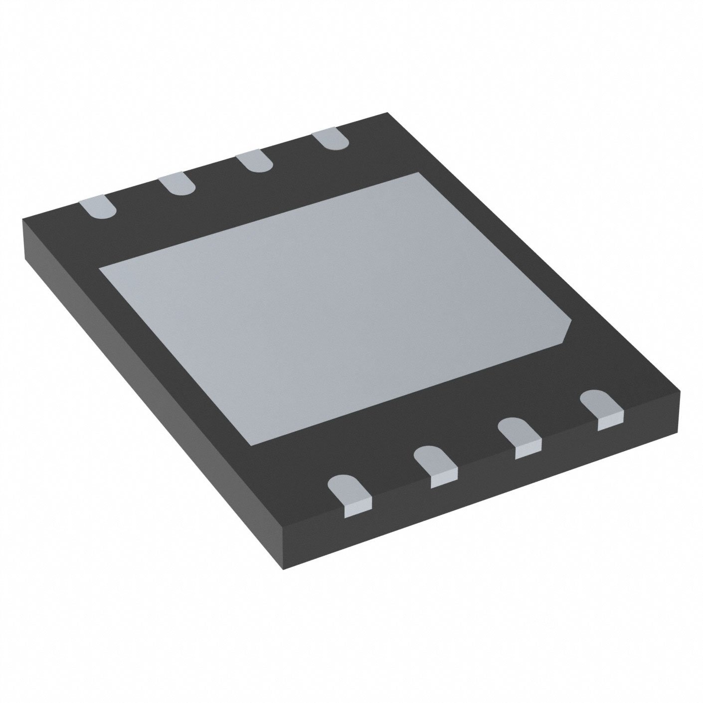
| Device Package | 48-WLCSP | Memory Format | FLASH | Technology | FLASH - NAND (SLC) | ||
|---|---|---|---|---|---|---|---|
| Memory Size | 512 Mbit | Access Time | 7 ns | Grade | Industrial | ||
| Clock Frequency | 104 MHz | Voltage | 1.7V ~ 1.95V | Memory Type | Non-Volatile | ||
| Operating Temperature | -40°C ~ 85°C (TA) | Write Cycle Time Word Page | 700 μs | Packaging | 48-UFBGA, WLCSP | ||
| Mounting Method | Non-Volatile | Memory Interface | SPI - Quad I/O | Memory Organization | 64M x 8 | ||
| Moisture Sensitivity Level | 1 (Unlimited) | RoHS Compliance | ROHS3 Compliant | REACH Compliance | REACH Unaffected | ||
| Qualification | N/A | ECCN | 3A991B1A | HTS Code | 8542.32.0071 |
Overview of W25N512GWYIT TR – IC FLASH 512MBIT SPI 48WLCSP
The W25N512GWYIT TR is a 1.8V, 512 M-bit serial SLC NAND flash memory implementing Dual/Quad SPI with buffer read and continuous read modes. It is organized as 64M x 8 and provides non-volatile storage in a compact 48-WLCSP / 48-UFBGA package.
Key device attributes from the datasheet include Quad I/O SPI interface, up to 104 MHz clock operation, a 7 ns access time, a 1.7 V–1.95 V supply range, and an operating temperature range of -40°C to 85°C. On-die features documented in the datasheet include protection and configuration registers, ECC support, bad block management, and standard SPI instruction support.
Key Features
- Memory Type & Capacity 512 Mbit SLC NAND flash organized as 64M x 8 for non-volatile data storage.
- Interface Serial SPI with Dual/Quad SPI and Quad I/O support for higher throughput over standard SPI links.
- Performance Clock frequency up to 104 MHz and 7 ns access time; supports buffer read and continuous read modes per the datasheet.
- Voltage and Power Low-voltage operation with a specified supply range of 1.7 V to 1.95 V (1.8 V class device).
- Program/Erase Timing Documented write cycle time (word/page) of 700 µs and support for block erase operations (128KB block erase described in the instruction set).
- Data Management & Protection On-chip protection and configuration registers, OTP-lockable bits (block protect, write protection enable, status lock), ECC enable/status bits, and bad block management with a BBM look-up table as detailed in the datasheet.
- Standard Instruction Set Supports common SPI instructions documented in the datasheet, including Read JEDEC ID and Read/Write Status Register commands.
- Package & Temperature Available in a 48-WLCSP (48-UFBGA) package; specified operating temperature range −40°C to 85°C (TA).
Unique Advantages
- High-density SLC NAND storage: 512 Mbit capacity (64M x 8) provides substantial non-volatile space while retaining SLC NAND characteristics as specified in the datasheet.
- Quad SPI throughput: Dual/Quad SPI and Quad I/O support combined with up to 104 MHz clocking enable higher serial read/write bandwidth within the documented interface limits.
- Low-voltage operation: Designed for 1.8 V systems with a defined supply window of 1.7 V–1.95 V to match low-voltage system requirements shown in the specifications.
- On-chip data management: Built-in protection registers, OTP-lockable configuration, ECC enable and ECC status reporting, and bad block management reduce the need for external management logic as described in the datasheet.
- Compact package: 48-WLCSP package option (48-UFBGA) provides a small form factor for board-level integration as indicated in the product specifications.
- Documented instruction support: Detailed instruction set coverage in the datasheet (Device ID, status registers, program/erase, continuous/buffer read modes) aids software integration and validation.
Why Choose IC FLASH 512MBIT SPI 48WLCSP?
The W25N512GWYIT TR positions itself as a 1.8 V SLC NAND serial flash memory offering a combination of high density and documented on-die management features. Its Quad I/O SPI interface, buffer/continuous read modes, and up to 104 MHz operation deliver a measured balance of throughput and low-voltage compatibility for systems that require sizable non-volatile storage.
With OTP-lockable protection bits, ECC support, bad block management, and a compact 48-WLCSP package, this device is suitable for designs where documented flash control, data integrity features, and small package footprint are priority design constraints. The provided instruction set and register descriptions in the datasheet facilitate integration and firmware development.
For pricing, availability, or to request a quote for the W25N512GWYIT TR, submit a sales inquiry or request a formal quote through your purchasing channel.