W9864G6JH-5
| Part Description |
IC DRAM 64MBIT PAR 54TSOP II |
|---|---|
| Quantity | 132 Available (as of June 13, 2026) |

| Product Category | Memory |
|---|---|
| Manufacturer | Winbond Electronics |
| Manufacturing Status | Obsolete |
| Manufacturer Standard Lead Time | Contact Us |
| Datasheet |
Specifications & Environmental
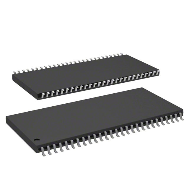
| Device Package | 54-TSOP II | Memory Format | DRAM | Technology | SDRAM | ||
|---|---|---|---|---|---|---|---|
| Memory Size | 64 Mbit | Access Time | 5 ns | Grade | Commercial | ||
| Clock Frequency | 200 MHz | Voltage | 3V ~ 3.6V | Memory Type | Volatile | ||
| Operating Temperature | 0°C ~ 70°C (TA) | Write Cycle Time Word Page | N/A | Packaging | 54-TSOP (0.400", 10.16mm Width) | ||
| Mounting Method | Volatile | Memory Interface | Parallel | Memory Organization | 4M x 16 | ||
| Moisture Sensitivity Level | 3 (168 Hours) | RoHS Compliance | ROHS Compliant | REACH Compliance | REACH Unaffected | ||
| Qualification | N/A | ECCN | EAR99 | HTS Code | 8542.32.0002 |
Overview of W9864G6JH-5 – IC DRAM 64MBIT PAR 54TSOP II
The W9864G6JH-5 from Winbond Electronics is a high-speed synchronous DRAM (SDRAM) device organized as 1M × 4 banks × 16 bits (4M × 16 total) delivering 64 Mbit of parallel memory. The -5 speed grade supports operation up to 200 MHz with CAS latency CL3 and is intended for designs that require parallel SDRAM memory with banked architecture and burst access modes.
This device supports standard SDRAM operation modes—including burst read/write, auto-precharge, self-refresh and power-down—and is offered in a 54-lead TSOP (II) package sized at 0.400" (10.16 mm) width, with recommended supply voltage between 3.0 V and 3.6 V and an operating ambient temperature range of 0 °C to 70 °C.
Key Features
- Core Architecture — Organized as 1M × 4 banks × 16 bits (4M × 16 total) to provide 64 Mbit of parallel SDRAM storage with banked access for interleaved operations.
- SDRAM Technology — Synchronous DRAM supporting burst modes, mode register set, and standard SDRAM command set for predictable timing and control behavior.
- Performance — -5 speed grade rated up to 200 MHz operation with CAS latency CL3 and an access time of 5 ns, enabling high-throughput burst transfers.
- Supported Operating Modes — Includes Bank Activate, Burst Read/Write, Auto-precharge, Precharge, Self Refresh, Power Down, No Operation and Clock Suspend as documented in the device functional description.
- Memory Interface — Parallel SDRAM interface suitable for systems requiring conventional SDRAM control and data signaling.
- Power — Supply voltage range of 3.0 V to 3.6 V to match typical 3 V SDRAM system rails.
- Package — 54-lead TSOP (II) package, 0.400" (10.16 mm) width, for space-efficient surface-mount mounting.
- Environmental Range — Specified operating ambient temperature range of 0 °C to 70 °C (TA).
Typical Applications
- Embedded systems — Parallel SDRAM storage for embedded controllers and subsystems that require banked memory and burst access.
- Consumer electronics — System memory for devices that need a 64 Mbit parallel SDRAM implemented in a compact TSOP (II) package.
- Industrial control equipment — Local volatile memory for control and buffering functions operating within the specified 0 °C to 70 °C ambient range.
Unique Advantages
- High data throughput: -5 speed grade supports operation up to 200 MHz/CL3 and a 5 ns access time for fast burst transfers.
- Banked architecture: 1M × 4 banks × 16 bits organization enables interleaved access patterns and improved effective concurrency.
- Comprehensive SDRAM feature set: Supports burst read/write, auto-precharge, self-refresh and power-down modes to suit varied power and timing requirements.
- Compact surface-mount package: 54-TSOP (II) footprint (0.400", 10.16 mm width) for dense board layouts.
- Standard parallel interface and voltage: 3.0 V to 3.6 V supply and conventional SDRAM signaling simplify integration into 3 V system designs.
Why Choose W9864G6JH-5?
The W9864G6JH-5 is positioned as a straightforward, high-speed SDRAM option for designs that require 64 Mbit of parallel volatile memory with banked operation and standard SDRAM control. Its -5 speed grade, support for common SDRAM commands and modes, and TSOP (II) packaging make it suitable for engineers seeking a compact memory device with documented timing and mode behavior.
This device is appropriate for product designs where predictable SDRAM timing, burst capability, and a 3.0 V–3.6 V supply are required. The combination of documented operating modes, banked architecture, and a compact package supports scalable integration into embedded, consumer, and industrial systems.
Request a quote or submit an inquiry for pricing and availability for the W9864G6JH-5 to receive detailed lead-time and ordering information.