W9864G6JT-6
| Part Description |
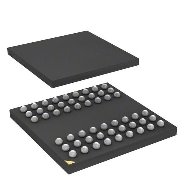
IC DRAM 64MBIT PARALLEL 54TFBGA |
|---|---|
| Quantity | 1,424 Available (as of June 9, 2026) |
| Product Category | Memory |
|---|---|
| Manufacturer | Winbond Electronics |
| Manufacturing Status | Obsolete |
| Manufacturer Standard Lead Time | Contact Us |
| Datasheet |
Specifications & Environmental
| Device Package | 54-TFBGA (8x8) | Memory Format | DRAM | Technology | SDRAM | ||
|---|---|---|---|---|---|---|---|
| Memory Size | 64 Mbit | Access Time | 5 ns | Grade | Commercial | ||
| Clock Frequency | 166 MHz | Voltage | 3V ~ 3.6V | Memory Type | Volatile | ||
| Operating Temperature | 0°C ~ 70°C (TA) | Write Cycle Time Word Page | N/A | Packaging | 54-TFBGA | ||
| Mounting Method | Volatile | Memory Interface | Parallel | Memory Organization | 4M x 16 | ||
| Moisture Sensitivity Level | 3 (168 Hours) | RoHS Compliance | ROHS Compliant | REACH Compliance | REACH Unaffected | ||
| Qualification | N/A | ECCN | EAR99 | HTS Code | 8542.32.0002 |
Overview of W9864G6JT-6 – IC DRAM 64MBIT PARALLEL 54TFBGA
The W9864G6JT-6 from Winbond Electronics is a 64‑Mbit synchronous DRAM (SDRAM) device organized as 1M × 4 banks × 16 bits (4M × 16) with a parallel memory interface. It implements burst‑oriented synchronous DRAM architecture and is specified for 166 MHz operation, delivering up to 166M words per second.
Engineered for systems that require compact, high‑speed volatile memory, the W9864G6JT-6 operates from a 3.0 V to 3.6 V supply and is provided in a 54‑ball TFBGA (8×8) package for board‑level integration within an ambient temperature range of 0°C to 70°C.
Key Features
- Memory Architecture Organized as 1M × 4 banks × 16 bits (4M × 16) to support parallel data paths and multi‑bank access.
- SDRAM, Burst‑Oriented Access Synchronous DRAM with burst access; supports programmable burst lengths including 1, 2, 4, 8 and full‑page mode (as documented in device operation).
- High‑Speed Operation Clock frequency rated at 166 MHz and specified to deliver data bandwidth up to 166M words per second; compliant to the 166 MHz/CL3 timing specification in the device documentation.
- Timing and Latency Access time specified at 5 ns with detailed timing and command sequences for read/write, bank activation, auto‑precharge, refresh and power modes defined in the datasheet.
- Power Single‑supply operation from 3.0 V to 3.6 V.
- Package 54‑TFBGA (8×8) compact ball‑grid package suitable for space‑efficient PCB implementations.
- Operating Conditions Ambient operating temperature specified as 0°C to 70°C (TA) for the -6 speed grade.
- Command and Control Full SDRAM command set and modes documented, including bank activate, burst read/write, auto‑precharge, self‑refresh, power‑down and clock suspend modes.
Typical Applications
- Parallel SDRAM memory subsystems Integration as a 64‑Mbit parallel SDRAM device where 166 MHz synchronous operation and burst access are required.
- Embedded systems requiring volatile high‑speed storage Use in designs that require a compact TFBGA footprint and a 3.0–3.6 V supply within 0°C–70°C ambient conditions.
- Multi‑bank burst data buffering Leverage the 1M × 4 bank organization for bank interleaving and burst‑oriented data transfers as described in the device documentation.
Unique Advantages
- 166 MHz rated throughput: Provides up to 166M words per second for applications constrained by synchronous parallel SDRAM bandwidth.
- Flexible burst control: Programmable burst lengths (1, 2, 4, 8, full page) enable tuning of sequential data transfers to match system requirements.
- Multi‑bank architecture: Four‑bank organization supports interleaved bank access patterns documented in the datasheet for improved access sequencing.
- Compact TFBGA package: 54‑ball TFBGA (8×8) helps minimize board space while providing standard ball‑out for assembly.
- Industry‑documented operation: Comprehensive command timing, power‑up/initialization and mode register programming are described in the manufacturer’s datasheet.
- Wide supply window: Operates across 3.0 V to 3.6 V to accommodate typical 3.3 V system rails.
Why Choose W9864G6JT-6?
The W9864G6JT-6 positions as a compact, high‑speed SDRAM option for designs needing a 64‑Mbit parallel memory with documented burst and multi‑bank operation at 166 MHz. Its combination of 1M × 4 bank organization, programmable burst lengths and full SDRAM command support provides design flexibility for synchronous memory subsystems.
This device is suitable for engineers and procurement teams seeking a Winbond‑documented SDRAM component in a 54‑TFBGA package, operating from 3.0 V to 3.6 V and specified for 0°C to 70°C ambient conditions.
Request a quote or contact sales to obtain pricing, lead time and availability for the W9864G6JT-6.