
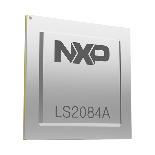
LS2084ASE7QQB
| Part Description |
ARM® Cortex®-A72 Microprocessor IC QorIQ® Layerscape 8 Core, 64-Bit 1.6GHz 1292-FCPBGA (37.5x37.5) |
|---|---|
| Quantity | 1,215 Available (as of October 8, 2026) |

| Product Category | Microprocessors |
|---|---|
| Part Series | LS2084A |
| Manufacturer | NXP USA Inc. |
| Manufacturing Status | Active |
| Manufacturer Standard Lead Time | 18 Weeks |
| Datasheet |
Specifications & Environmental
| Core Processor | ARM® Cortex®-A72 | Device Package | 1292-FCPBGA (37.5x37.5) | ECCN | N/A | ||
|---|---|---|---|---|---|---|---|
| Ethernet | 10GbE (8), 2.5GbE (16) | HTS Code | N/A | Moisture Sensitivity Level | 3 (168 Hours) | ||
| Mounting Method | Surface Mount | Mounting Type | Surface Mount | Number of Cores/Bus Width | 8 Core, 64-Bit | ||
| Operating Temperature | 0°C ~ 105°C (TA) | Package / Case | 1292-BBGA, FCBGA | RAM Controllers | DDR4 | ||
| REACH Compliance | REACH Unaffected | RoHS Compliance | ROHS3 Compliant | SATA | SATA (2) | ||
| Security Features | Secure Boot, TrustZone® | Speed | 1.6GHz | Supplier Device Package | 1292-FCPBGA (37.5×37.5) | ||
| USB | USB 3.0 + PHY (2) |
Overview of LS2084ASE7QQB – IC MPU QORIQ 1.6GHZ 1292FCPBGA
The LS2084ASE7QQB is an NXP Semiconductors QorIQ Layerscape microprocessor featuring an 8-core ARM® Cortex®-A72 64-bit architecture running at 1.6 GHz. Designed for embedded and networking-focused applications, this device integrates high-throughput I/O, datapath acceleration, and multi-core processing to support demanding packet-processing and compute tasks.
With on-chip memory controllers, extensive Ethernet connectivity, and hardware acceleration engines from the Layerscape family, the LS2084ASE7QQB targets systems that require scalable performance, secure boot and partitioning, and robust platform integration.
Key Features
- CPU Core Architecture Eight ARM® Cortex®-A72 cores (64-bit) arranged for multi-core performance at a 1.6 GHz operating frequency.
- Cache and Interconnect Platform-level cache and hierarchical interconnect fabric provide low-latency data paths and coherent multi-core operation; series documentation references 1 MB platform cache with ECC protection.
- Memory Subsystem Dual 64-bit DDR4 SDRAM memory controllers with ECC and interleaving support for high-bandwidth system memory.
- Datapath Acceleration (DPAA2) Integrated datapath acceleration architecture including a wire-rate IO processor (WRIOP), queue and buffer management, cryptography acceleration (SEC 5.2), RegEx pattern matching (PME 2.0), and compression/decompression (DCE 1.0) for accelerated packet and data processing workloads.
- High-Speed SerDes and PCIe 16 SerDes lanes and four PCIe 3.0 controllers (supporting multiple lane widths) to connect high-bandwidth peripherals and offload engines.
- Extensive Ethernet Connectivity Hardware supports up to eight 10 GbE MACs and up to sixteen 1/2.5 GbE MACs, enabling high-density networking ports and aggregation designs.
- Peripheral Interfaces Two SATA 3.0 controllers and two USB 3.0 controllers with integrated PHYs, plus SPI/QSPI, I2C, DUARTs and an integrated flash controller for flexible peripheral integration.
- Security and Virtualization Secure Boot and ARM TrustZone® support combined with hardware virtualization and partitioning enforcement for platform security and workload isolation.
- Package and Thermal Supplied in a 1292-ball FCPBGA package (37.5 × 37.5 mm) suitable for surface-mount assembly; operating temperature range 0 °C to 105 °C.
- Compliance RoHS compliant.
Typical Applications
- Network Infrastructure High-density routing, switching and aggregation platforms that require multiple 10 GbE and 2.5 GbE interfaces and hardware packet acceleration.
- Security and VPN Appliances Appliances leveraging on-chip cryptography acceleration and TrustZone® for secure data-plane processing and secure boot workflows.
- Edge Compute and Telecom Edge devices and telecommunications equipment that need multi-core processing, PCIe connectivity, and accelerated data-path functions for low-latency services.
- Storage and Interface Gateways Systems combining SATA, high-speed PCIe peripherals and USB 3.0 for storage aggregation, gateway and appliance roles.
Unique Advantages
- Multi-core ARM® Cortex®-A72 performance: Eight 64-bit cores deliver parallel compute capacity for control-plane and data-plane tasks.
- Integrated datapath acceleration: DPAA2 engines offload packet parsing, queue management and cryptography to reduce CPU load and improve throughput.
- Comprehensive connectivity: Large counts of 10 GbE and 2.5 GbE MACs plus PCIe and SerDes lanes simplify system design for high-bandwidth applications.
- Memory reliability: DDR4 controllers with ECC and interleaving support improve resilience for memory-intensive workloads.
- Secure platform features: Secure Boot, TrustZone® and a service processor for pre-boot initialization enable secure system bring-up and runtime isolation.
- Compact high-density package: 1292-FCPBGA (37.5 × 37.5 mm) provides a high-pin-count solution for complex embedded boards.
Why Choose LS2084ASE7QQB?
The LS2084ASE7QQB positions itself as a high-capacity Layerscape MPU for embedded networking and compute applications that demand multi-core ARM® performance, extensive I/O, and dedicated datapath acceleration. Its combination of DDR4 memory controllers with ECC, large Ethernet MAC counts, PCIe connectivity and hardware acceleration engines makes it well suited for systems that require both packet-handling throughput and secure, isolated execution.
Engineers designing routers, security appliances, edge compute nodes or storage gateways will find the LS2084ASE7QQB offers a balanced integration of processing, acceleration and peripheral interfaces to simplify board-level design while addressing performance and reliability requirements.
Request a quote or submit an inquiry to receive pricing and availability for the LS2084ASE7QQB.


















Date Founded: 2006
Headquarters: Eindhoven, North Brabant, Netherlands
Employees: 38,000+
Revenue: $10.53 Billion
Certifications and Memberships: ISO9001:2015, IATF16949:2016


