
LS2088ASN7V1B
| Part Description |
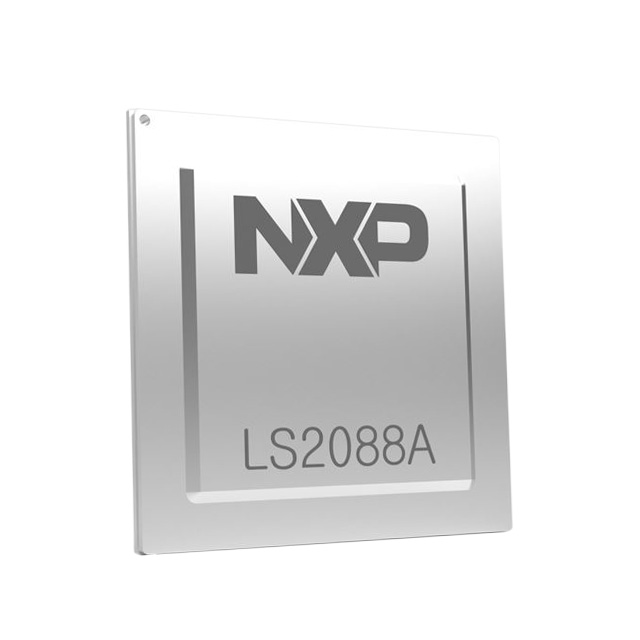
ARM® Cortex®-A72 Microprocessor IC QorIQ® Layerscape 8 Core, 64-Bit 2.0GHz 1292-FCPBGA (37.5x37.5) |
|---|---|
| Quantity | 952 Available (as of October 8, 2026) |
| Product Category | Microprocessors |
|---|---|
| Part Series | LS2088A |
| Manufacturer | NXP USA Inc. |
| Manufacturing Status | Active |
| Manufacturer Standard Lead Time | 18 Weeks |
| Datasheet |
Specifications & Environmental
| Core Processor | ARM® Cortex®-A72 | Device Package | 1292-FCPBGA (37.5x37.5) | ECCN | 3A991A2 | ||
|---|---|---|---|---|---|---|---|
| Ethernet | 10GbE (8) or 1GbE (16) & 2.5GbE (1) | HTS Code | 8542.31.0001 | Moisture Sensitivity Level | 3 (168 Hours) | ||
| Mounting Method | Surface Mount | Mounting Type | Surface Mount | Number of Cores/Bus Width | 8 Core, 64-Bit | ||
| Operating Temperature | 0°C ~ 105°C | Package / Case | 1292-BFBGA, FCBGA | RAM Controllers | DDR4 | ||
| REACH Compliance | REACH Unaffected | RoHS Compliance | ROHS3 Compliant | SATA | SATA 6Gbps (2) | ||
| Speed | 2.0GHz | Supplier Device Package | 1292-FCPBGA (37.5×37.5) | USB | USB 3.0 (2) + PHY |
Overview of LS2088ASN7V1B – ARM Cortex-A72 8‑Core 2.0GHz
The LS2088ASN7V1B is an NXP QorIQ Layerscape microprocessor IC featuring up to eight 64‑bit ARM® Cortex®‑A72 cores running at 2.0 GHz in a 1292‑FCPBGA (37.5×37.5 mm) package. It is designed for high‑performance embedded networking and control applications that require multi‑core compute and extensive packet‑processing capabilities.
Targeted use cases include enterprise SDN switching, network‑function virtualization (NFV), cloud and data center switching, and wireless cell‑site routing. Integrated packet processing, a Layer‑2 switch architecture and a comprehensive software board support package deliver an implementation path focused on performance, efficiency and system integration.
Key Features
- Core Architecture ARM® Cortex®‑A72 based 64‑bit processor up to 2.0 GHz with up to eight cores for parallel compute and control tasks.
- Memory Support DDR4 memory controller support; reference design details include dual‑rank DDR4 uDIMM support with x72 data paths, per‑slot capacities and ECC enablement for reliable system memory.
- High‑Speed Networking Flexible Ethernet options: support for up to eight 10 GbE ports or combinations such as sixteen 1 GbE plus one 2.5 GbE, together with an integrated Layer‑2 switch and DPAA2 packet‑processing architecture.
- Storage & I/O SATA 6 Gbps (2 ports), two USB 3.0 ports with PHY, and PCIe expansion support (including x8 Gen3 or split configurations) for storage and peripheral flexibility.
- Packet Processing & Management Advanced packet processor and DPAA2 architecture with L2 switch objects and a management complex to simplify programming of networking functions.
- Software & Development Reference designs ship with a Linux‑based BSP, U‑Boot boot loader, DPAA2 kernel support and NADK user‑space components to accelerate networking application development.
- Security Secure Boot and ARM TrustZone® support to help establish a hardware root of trust and isolate secure execution domains.
- Package & Thermal 1292‑FCPBGA package (37.5×37.5 mm) in a surface‑mount format; specified operating temperature range 0 °C to 105 °C.
- Compliance RoHS‑compliant construction.
Typical Applications
- SDN/OpenFlow Switching Implements control and data‑plane functions with integrated L2 switching and DPAA2 packet processing for software‑defined networking deployments.
- Network‑Function Virtualization (NFV) Hosts virtualized network services and control‑plane workloads using multi‑core compute and Linux BSP support for rapid NFV development.
- Data Center & Cloud Switching Provides high‑throughput interfaces and packet acceleration features suitable for top‑of‑rack or aggregation switching in cloud environments.
- Wireless Cell‑Site Routing Enables routing and control functions at wireless sites with multi‑core processing, high‑speed Ethernet and robust I/O options.
Unique Advantages
- Multi‑Core Compute and Scale: Eight 64‑bit Cortex‑A72 cores at 2.0 GHz deliver compute headroom for control planes, management tasks and parallel packet processing.
- Integrated Packet Processing: DPAA2 architecture and an autonomous packet processor plus L2 switch objects reduce software complexity for networking workloads.
- Comprehensive I/O Mix: Multiple 10 GbE/1 GbE/2.5 GbE options, SATA 6 Gbps, USB 3.0 and PCIe provide flexible system partitioning for networking, storage and expansion.
- Software Ecosystem: Linux BSP, U‑Boot and NADK user‑space components accelerate time‑to‑market for embedded networking applications.
- Security Foundations: Secure Boot and TrustZone® support help enable secure device boot and isolated execution environments.
- Component Readiness: Surface‑mount 1292‑FCPBGA package and RoHS compliance simplify manufacturing and regulatory alignment.
Why Choose LS2088ASN7V1B?
The LS2088ASN7V1B positions itself as a performance‑oriented, highly integrated processor for embedded networking and control systems where multi‑core compute, packet processing and flexible I/O are required. Its combination of eight Cortex‑A72 cores, DPAA2 packet architecture and a broad set of interfaces supports demanding SDN, NFV and routing designs.
Designed with a Linux BSP and development tools in the reference design, this device is suitable for engineers building scalable, software‑driven network equipment and appliances that require a clear upgrade path and ecosystem support from NXP.
Request a quote or submit a request for pricing and availability to begin evaluation and integration of the LS2088ASN7V1B into your next networking or embedded design.



















Date Founded: 2006
Headquarters: Eindhoven, North Brabant, Netherlands
Employees: 38,000+
Revenue: $10.53 Billion
Certifications and Memberships: ISO9001:2015, IATF16949:2016


