
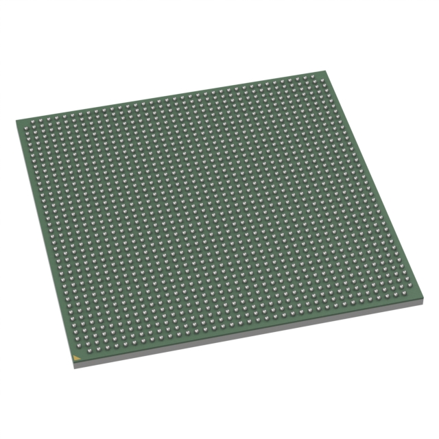
LX2080SE72029B
| Part Description |
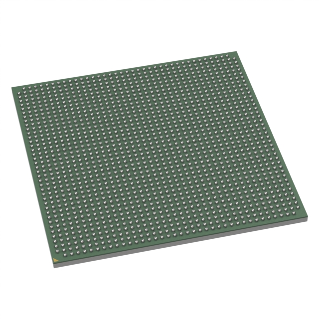
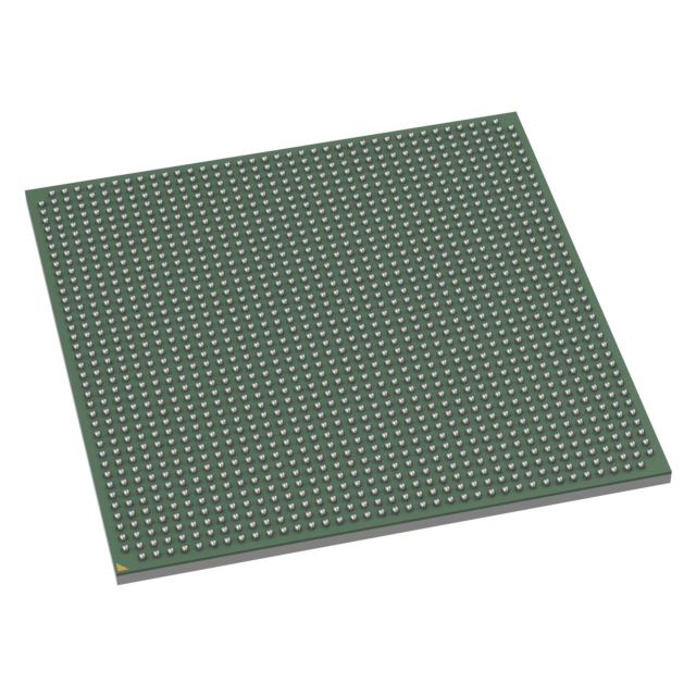
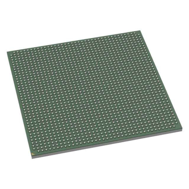
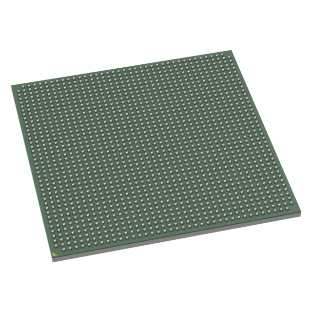
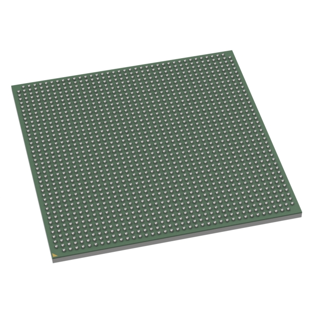
ARM® Cortex®-A72 Microprocessor IC QorlQ LX2 8 Core, 64-Bit 2GHz 1517-FCPBGA (40x40) |
|---|---|
| Quantity | 614 Available (as of October 8, 2026) |
| Product Category | Microprocessors |
|---|---|
| Part Series | LX2080S |
| Manufacturer | NXP USA Inc. |
| Manufacturing Status | Active |
| Manufacturer Standard Lead Time | 18 Weeks |
| Datasheet |
Specifications & Environmental
| Core Processor | ARM® Cortex®-A72 | Device Package | 1517-FCPBGA (40x40) | ECCN | N/A | ||
|---|---|---|---|---|---|---|---|
| Ethernet | 100Gbps (2) | Graphics Acceleration | Yes | HTS Code | N/A | ||
| Moisture Sensitivity Level | N/A | Mounting Method | Surface Mount | Mounting Type | Surface Mount | ||
| Number of Cores/Bus Width | 8 Core, 64-Bit | Operating Temperature | 0°C ~ 105°C (TJ) | Package / Case | 1517-BBGA, FCBGA | ||
| RAM Controllers | DDR4 | REACH Compliance | REACH Unaffected | RoHS Compliance | ROHS3 Compliant | ||
| SATA | SATA 3.0 (4) | Security Features | Secure Boot, TrustZone® | Speed | 2GHz | ||
| Supplier Device Package | 1517-FCPBGA (40×40) | USB | USB 3.0 (2) + PHY (2) | Voltage – I/O | 1.2V, 1.8V, 3.3V |
Overview of LX2080SE72029B – IC MPU QorlQ LX2 8‑Core 2 GHz, 1517‑FCPBGA
The LX2080SE72029B is an NXP Layerscape LX2080S series microprocessor IC featuring an 8‑core, 64‑bit ARM® Cortex®‑A72 architecture running at 2 GHz. Designed for embedded and networking applications, it combines multi‑core compute with a broad set of on‑chip interfaces to simplify high‑bandwidth system designs.
With integrated DDR4 memory controllers, multi‑100GbE capable Ethernet, multiple SATA and USB channels, and hardware security primitives, this device targets compute‑intensive embedded networking, edge processing and telecom applications that require both performance and a compact surface‑mount package.
Key Features
- Core & Performance ARM® Cortex®‑A72 64‑bit core processor, 8 cores running at 2 GHz for multi‑threaded embedded workloads.
- Memory DDR4 RAM controller support to enable high bandwidth system memory for packet buffering and application tasks.
- High‑Speed Networking Dual 100 Gbps Ethernet interfaces (2) to support high throughput networking and telecom use cases.
- Storage & USB Four SATA 3.0 ports and two USB 3.0 ports plus two USB PHYs for flexible storage and peripheral connectivity.
- Security Secure Boot and Arm TrustZone® support to help protect boot integrity and create trusted execution environments.
- Additional Interfaces CANbus support and graphics acceleration capability provide options for control networks and display/acceleration tasks.
- Package & Mounting 1517‑FCPBGA (40 × 40 mm) surface‑mount package for compact, high‑density board designs.
- Operating Range & Compliance Operating temperature 0 °C to 105 °C and RoHS compliant for standard commercial/industrial embedded deployments.
- Qualification Classified as Consumer qualification for non‑automotive embedded products.
Typical Applications
- Networking & Telecom — Use dual 100 Gbps Ethernet and multi‑core processing for control‑plane or data‑plane tasks in network appliances and edge routers.
- Edge & Industrial Processing — DDR4 memory support, CANbus, and extended operating temperature enable protocol handling and control tasks at the network edge.
- Storage Gateways — Multiple SATA 3.0 ports and USB 3.0 interfaces support high‑performance local storage and media handling in gateway and appliance designs.
- 5G & Packet Processing — Multi‑core CPU and high‑speed I/O address the throughput needs of packet processing and edge telecom functions.
Unique Advantages
- Multi‑core ARM performance: Eight Cortex‑A72 cores at 2 GHz deliver scalable compute for parallel embedded workloads and networking tasks.
- Broad, high‑speed I/O set: Dual 100 Gbps Ethernet ports, SATA and USB interfaces reduce external bridging and simplify system BOM.
- Built‑in security primitives: Secure Boot and TrustZone® support help protect platform integrity and enable trusted execution.
- Compact surface‑mount package: 1517‑FCPBGA (40×40) format enables dense PCB layouts for space‑constrained appliance designs.
- RoHS compliance: Environmentally compliant manufacturing footprint for global commercial deployment.
- Flexible connectivity: CANbus and graphics acceleration options broaden application possibilities from control networks to accelerated data paths.
Why Choose LX2080SE72029B?
The LX2080SE72029B positions itself as a high‑performance, highly integrated Layerscape microprocessor for embedded networking and edge systems. It balances multi‑core compute, extensive high‑speed I/O, and hardware security features in a compact FCPBGA package to help reduce board complexity and accelerate time to market.
This part is suited to engineering teams building networking appliances, edge gateways, or telecom edge systems that require deterministic performance, wide connectivity, and hardware‑level security. As part of the NXP Layerscape family, it aligns with established processor toolchains and resources for embedded development.
Request a quote or submit an inquiry to receive pricing, availability, and technical assistance for LX2080SE72029B. Our team can help evaluate fit for your design and provide next steps for procurement.



















Date Founded: 2006
Headquarters: Eindhoven, North Brabant, Netherlands
Employees: 38,000+
Revenue: $10.53 Billion
Certifications and Memberships: ISO9001:2015, IATF16949:2016


