
MC68360ZP25L
| Part Description |
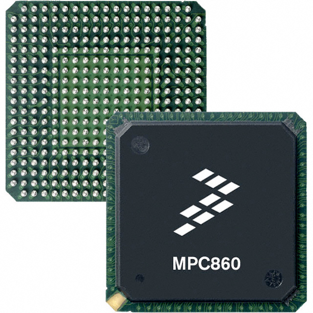
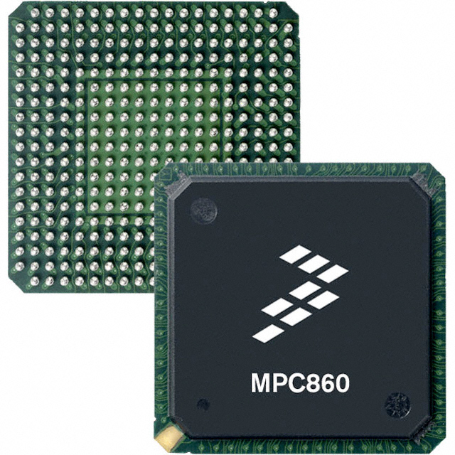
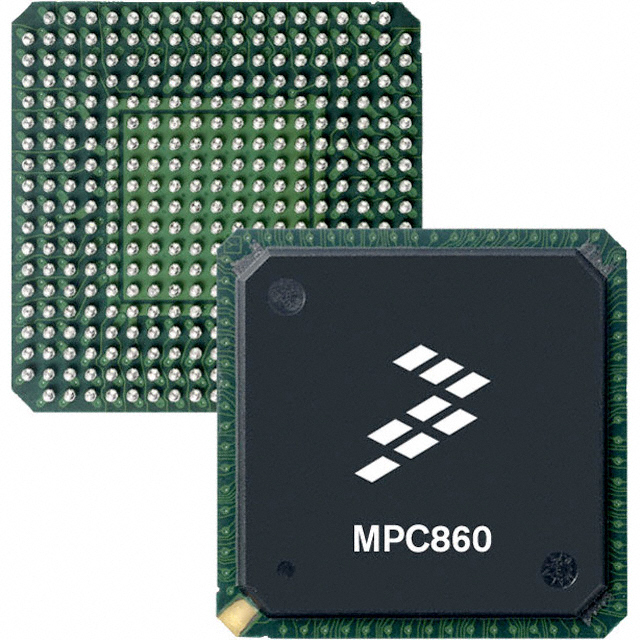
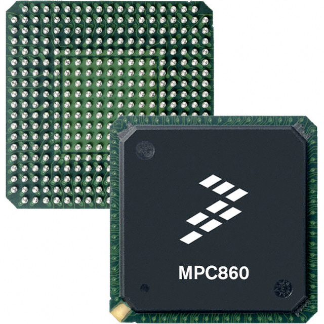
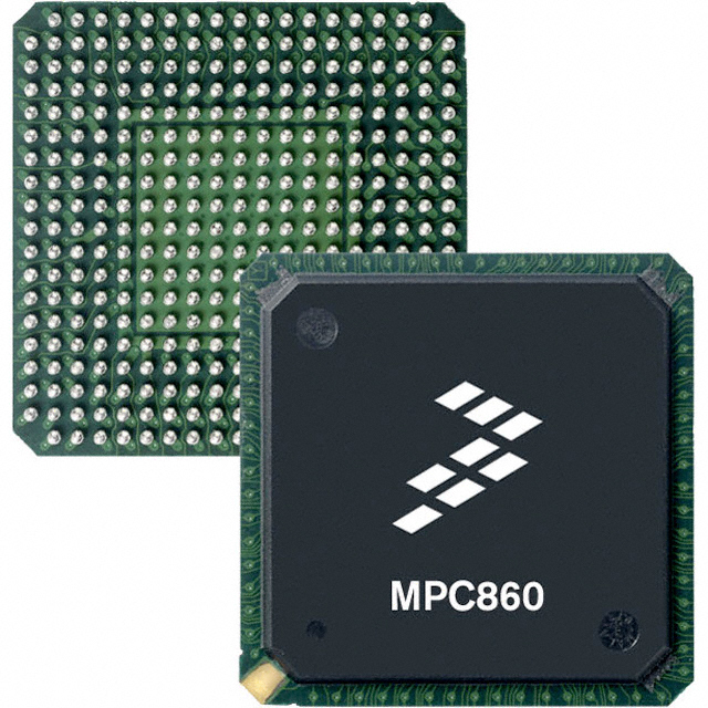
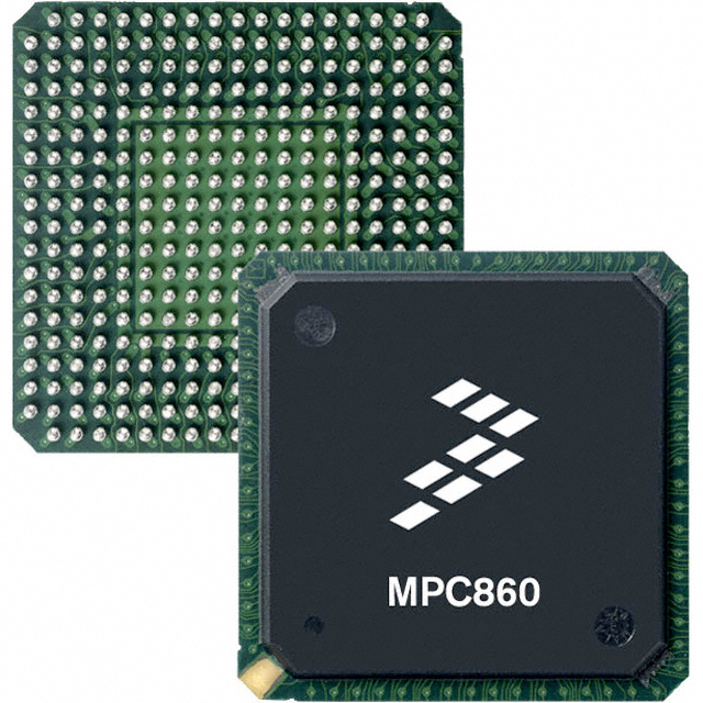
CPU32+ Microprocessor IC M683xx 1 Core, 32-Bit 25MHz 357-PBGA (25x25) |
|---|---|
| Quantity | 645 Available (as of October 8, 2026) |
| Product Category | Microprocessors |
|---|---|
| Part Series | MC68360 |
| Manufacturer | NXP USA Inc. |
| Manufacturing Status | Obsolete |
| Manufacturer Standard Lead Time | Contact Us |
| Datasheet |
Specifications & Environmental
| Co-Processors/DSP | Communications; CPM | Core Processor | CPU32+ | Device Package | 357-PBGA (25x25) | ||
|---|---|---|---|---|---|---|---|
| ECCN | EAR99 | Ethernet | 10Mbps (1) | Graphics Acceleration | No | ||
| HTS Code | 8542.31.0001 | Moisture Sensitivity Level | 3 (168 Hours) | Mounting Method | Surface Mount | ||
| Mounting Type | Surface Mount | Number of Cores/Bus Width | 1 Core, 32-Bit | Operating Temperature | 0°C ~ 70°C (TA) | ||
| Package / Case | 357-BGA | RAM Controllers | DRAM | REACH Compliance | REACH Unaffected | ||
| RoHS Compliance | RoHS non-compliant | Speed | 25MHz | Supplier Device Package | 357-PBGA (25×25) | ||
| Voltage – I/O | 5.0V |
Overview of MC68360ZP25L – IC MPU M683XX 25MHZ 357BGA
The MC68360ZP25L is a CPU32+ microprocessor from NXP Semiconductors' MC68360 series, implementing a single 32‑bit CPU32+ core running at 25 MHz. It is built on the QUICC (QUad Integrated Communications Controller) architecture and integrates communications-focused subsystems for embedded designs.
Targeted at embedded communications and control applications, the device combines a Communications Processor Module (CPM), DRAM controller, serial communications channels (SCC), and a 10 Mbps Ethernet interface to support networked embedded systems and communications equipment. The device is supplied in a 357‑PBGA (25×25) surface‑mount package and is RoHS compliant.
Key Features
- CPU32+ 32‑bit Core — Single 32‑bit CPU32+ core running at 25 MHz for deterministic embedded processing.
- QUICC Communications Architecture — Based on the MC68360 QUICC family with an integrated Communications Processor Module (CPM) and System Integration Module (SIM60) referenced in the device documentation.
- Integrated Communications Engines — Co‑processor support for communications (CPM) and serial channel interfaces (SCC) for protocol and serial data handling.
- DRAM Controller — On‑chip support for DRAM to enable external memory interfacing for buffering and application code storage.
- 10 Mbps Ethernet — Single Ethernet interface supporting 10 Mbps connectivity for networked applications.
- 5 V I/O — Device I/O referenced to 5 V for compatibility with legacy embedded systems.
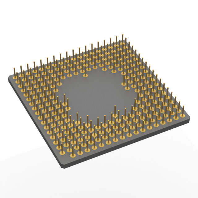
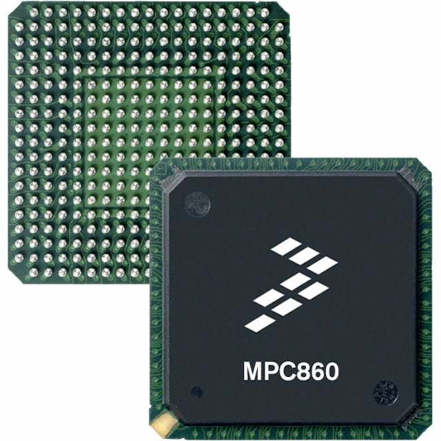
- Package & Mounting — 357‑PBGA (25×25) package, surface mount for compact board integration.
- Operating Range — Specified operating temperature from 0 °C to 70 °C for standard commercial environments.
- RoHS Compliant — Meets RoHS environmental compliance requirements.
Typical Applications
- Embedded Communications Control — Use the integrated CPM and SCC resources to implement protocol handling and serial communications in embedded systems.
- Networked Embedded Systems — The on‑chip 10 Mbps Ethernet interface and DRAM controller enable network connectivity and local buffering for devices on legacy Ethernet segments.
- Industrial and Telecom Equipment — QUICC architecture and communications co‑processing suit the device for communication‑centric control functions in industrial and telecom gear.
- Memory‑Assisted Applications — DRAM controller support allows designs that require external memory for runtime data and code storage.
Unique Advantages
- Communications‑Focused Integration: Built‑in CPM and SCC interfaces reduce external component needs for serial and communications tasks.
- Deterministic 32‑Bit Processing: CPU32+ single‑core 32‑bit architecture at 25 MHz provides predictable performance for embedded control loops and protocol stacks.
- On‑Chip Memory Controller: DRAM controller simplifies memory subsystem design and supports larger buffering for networking workloads.
- Legacy Network Support: Native 10 Mbps Ethernet enables direct integration into existing 10BASE‑T infrastructure.
- Commercial Temperature and 5 V I/O: Specification for 0 °C to 70 °C operation and 5 V I/O makes it compatible with many standard embedded platforms.
- Compact Surface‑Mount Package: 357‑PBGA (25×25) format supports high‑density board layouts while remaining manufacturable with standard SMT processes.
Why Choose MC68360ZP25L?
The MC68360ZP25L positions itself as a communications‑centric, integrated microprocessor solution within the MC68360 series. Its CPU32+ core, CPM communications engine, DRAM controller, SCC interfaces, and 10 Mbps Ethernet combine to address embedded designs that require on‑chip communications processing and external memory support in a compact 357‑PBGA package.
This device is suited to engineers developing networked embedded controllers, communications equipment, or industrial systems operating in commercial temperature environments who require a solution with built‑in communications peripherals and standard 5 V I/O. RoHS compliance and the QUICC architectural lineage add to long‑term design consistency and ecosystem support.
Request a quote or submit an RFQ to receive pricing, availability, and lead‑time information for the MC68360ZP25L.





















Date Founded: 2006
Headquarters: Eindhoven, North Brabant, Netherlands
Employees: 38,000+
Revenue: $10.53 Billion
Certifications and Memberships: ISO9001:2015, IATF16949:2016


