
MC68360VR25VL
| Part Description |
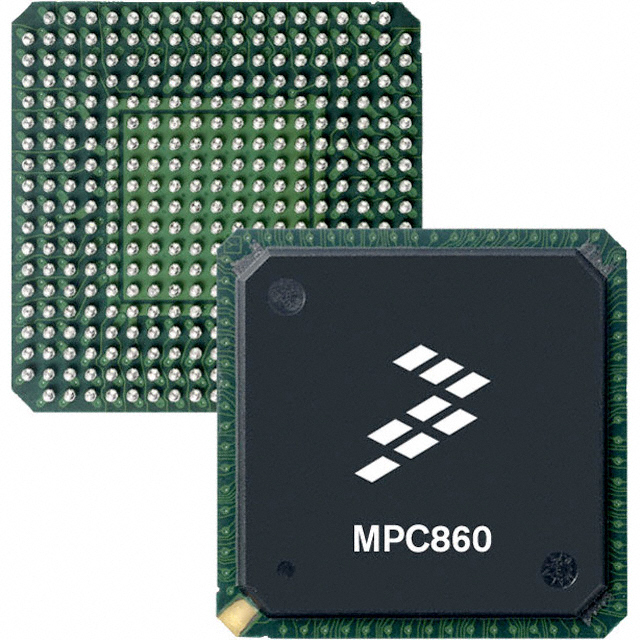
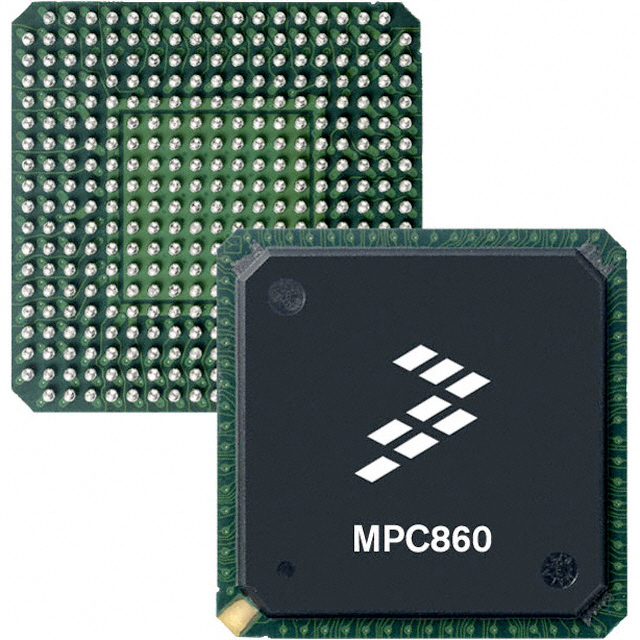
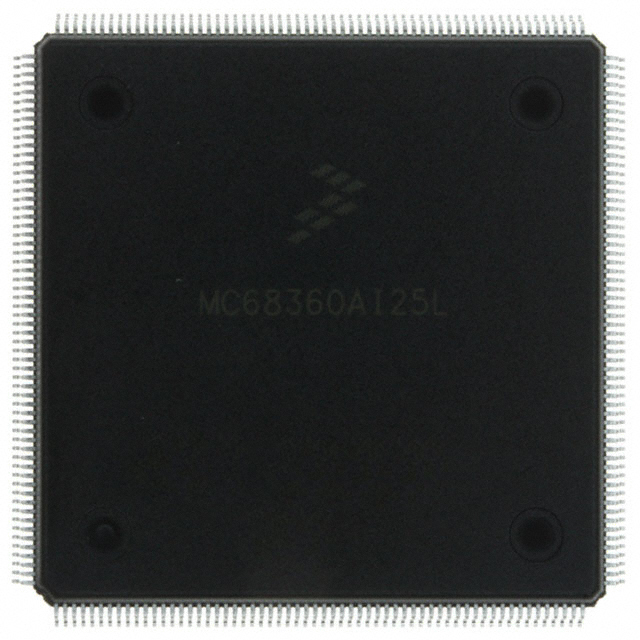
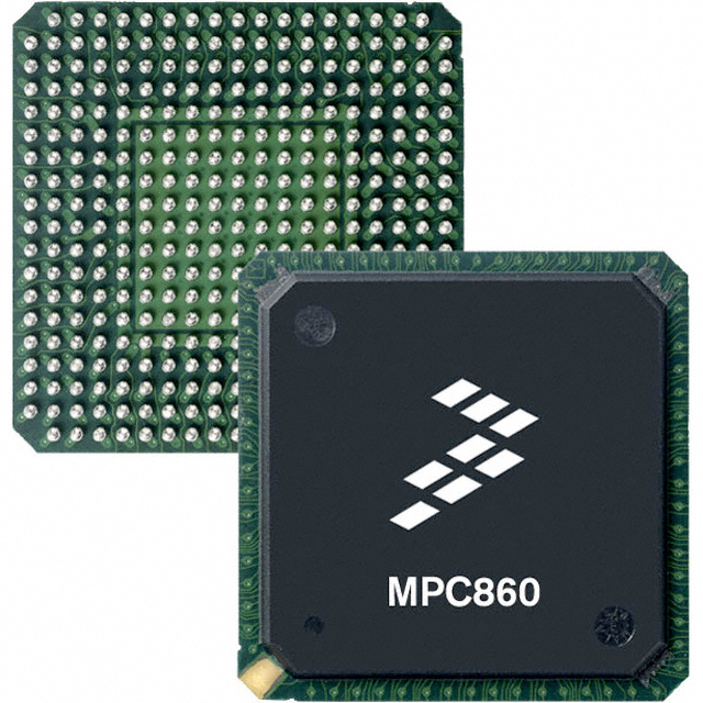
CPU32+ Microprocessor IC M683xx 1 Core, 32-Bit 25MHz 357-PBGA (25x25) |
|---|---|
| Quantity | 1,364 Available (as of October 8, 2026) |
| Product Category | Microprocessors |
|---|---|
| Part Series | MC68360 |
| Manufacturer | NXP USA Inc. |
| Manufacturing Status | Obsolete |
| Manufacturer Standard Lead Time | Contact Us |
| Datasheet |
Specifications & Environmental
| Co-Processors/DSP | Communications; CPM | Core Processor | CPU32+ | Device Package | 357-PBGA (25x25) | ||
|---|---|---|---|---|---|---|---|
| ECCN | EAR99 | Ethernet | 10Mbps (1) | Graphics Acceleration | No | ||
| HTS Code | 8542.31.0001 | Moisture Sensitivity Level | 3 (168 Hours) | Mounting Method | Surface Mount | ||
| Mounting Type | Surface Mount | Number of Cores/Bus Width | 1 Core, 32-Bit | Operating Temperature | 0°C ~ 70°C (TA) | ||
| Package / Case | 357-BBGA | RAM Controllers | DRAM | REACH Compliance | REACH Unaffected | ||
| RoHS Compliance | ROHS3 Compliant | Speed | 25MHz | Supplier Device Package | 357-PBGA (25×25) | ||
| Voltage – I/O | 3.3V |
Overview of MC68360VR25VL – IC MPU M683XX 25MHZ 357BGA
The MC68360VR25VL is a CPU32+ based microprocessor in the MC68360 QUICC family, offering a single 32‑bit core running at 25 MHz in a 357‑PBGA (25×25) surface‑mount package. It combines a CPU32+ core with an integrated Communications Processor Module (CPM) and multiple serial controllers, making it well suited for embedded controller designs with a focus on communications tasks.
Designed for controller and communications applications, the device integrates bus, memory and peripheral features to simplify system design while supporting common serial and network interfaces used in embedded systems.
Key Features
- Core CPU32+ single 32‑bit core running at 25 MHz; CPU32+ is functionally compatible with CPU32 and supports background debug mode and byte‑misaligned addressing (as documented for the MC68360 series).
- Memory and Bus Up to 32‑bit data bus with dynamic bus sizing for 8‑ and 16‑bit operation; boot chip select available at reset and support for SRAM/EPROM/Flash memory configurations referenced for the series.
- Communications Processor (CPM) On‑chip CPM (RISC controller) with series‑level features such as buffer descriptors and continuous mode transmit/receive to offload serial protocol handling.
- Serial and Network Interfaces Four serial communications controllers (SCCs), two serial management controllers (SMCs) and one SPI channel as part of the QUICC architecture; Ethernet 10 Mbps available on SCC1 (series option) and HDLC/SDLC support.
- DMA and Timers Two independent DMA channels with buffer chaining and auto buffer modes; four general‑purpose timers configurable as four 16‑bit timers or two 32‑bit timers.
- System Integration Module (SIM60) Integrated system functions including watchdog, periodic interrupt timer, clock synthesizer, bus/error monitors and low power stop mode (series features).
- Package and Power Supplier device package: 357‑PBGA (25×25), surface mount; I/O voltage: 3.3 V; operational speed: 25 MHz.
- Environmental and Operating Range Commercial temperature rating with an operating range of 0 °C to 70 °C and RoHS compliance.
Typical Applications
- Embedded Communications Modules Offload and manage serial and network protocols using the integrated CPM and multiple SCC/SMC channels.
- Industrial Controller Interfaces Implement protocol handling, serial link bridging and peripheral control in industrial embedded systems within the 0 °C to 70 °C range.
- Networked Embedded Products Integrate 10 Mbps Ethernet (series option on SCC1) and multi‑channel serial support for localized network interfaces and device connectivity.
Unique Advantages
- Highly integrated communications peripherals: The QUICC architecture combines CPU32+ and a CPM with multiple SCCs/SMCs to reduce external logic and simplify protocol implementations.
- Offloadable protocol processing: The CPM and buffer descriptor support enable continuous mode transmission/reception and relieve the main CPU from low‑level serial handling.
- Flexible memory and bus support: Up to 32‑bit data bus with dynamic sizing and boot chip select options simplifies memory subsystem design for a range of memory widths.
- On‑chip system monitoring and power features: SIM60 provides watchdog, periodic interrupts, bus monitors and a low power stop mode to assist system reliability and power management.
- Compact surface‑mount package: 357‑PBGA (25×25) package provides a high‑density footprint for space‑constrained board designs.
- Commercial temperature and RoHS compliant: Suitable for commercial embedded applications with RoHS compliance for environmental requirements.
Why Choose MC68360VR25VL?
MC68360VR25VL positions itself as a single‑chip communications‑focused microprocessor solution that combines a CPU32+ core with an integrated CPM and multiple serial controllers. The device is aimed at embedded designs that require on‑chip protocol acceleration, flexible memory interfacing and a compact PBGA package.
Backed by NXP Semiconductors' MC68360 QUICC architecture, the part is appropriate for engineers building communication‑centric embedded controllers, network interfaces or industrial controller modules who need integrated peripherals and predictable commercial operating ranges.
Request a quote or submit an inquiry to obtain pricing and availability for MC68360VR25VL and to discuss how it fits your embedded communications design requirements.





















Date Founded: 2006
Headquarters: Eindhoven, North Brabant, Netherlands
Employees: 38,000+
Revenue: $10.53 Billion
Certifications and Memberships: ISO9001:2015, IATF16949:2016


