
10AX027E2F27I2SG
| Part Description |
Arria 10 GX Field Programmable Gate Array (FPGA) IC 240 17870848 270000 672-BBGA, FCBGA |
|---|---|
| Quantity | 161 Available (as of June 18, 2026) |

| Product Category | Field Programmable Gate Array (FPGA) |
|---|---|
| Manufacturer | Intel |
| Manufacturing Status | Active |
| Manufacturer Standard Lead Time | 16 Weeks |
| Datasheet |
Specifications & Environmental
| Device Package | 672-FBGA, FC (27x27) | Grade | Industrial | Operating Temperature | -40°C – 100°C | ||
|---|---|---|---|---|---|---|---|
| Package / Case | 672-BBGA, FCBGA | Number of I/O | 240 | Voltage | 870 mV - 980 mV | ||
| Mounting Method | Surface Mount | RoHS Compliance | RoHS Compliant | REACH Compliance | REACH Unaffected | ||
| Moisture Sensitivity Level | 3 (168 Hours) | Number of LABs/CLBs | 101620 | Number of Logic Elements/Cells | 270000 | ||
| Number of Gates | N/A | ECCN | 5A002A1 | HTS Code | 8542.39.0001 | ||
| Qualification | N/A | Total RAM Bits | 17870848 |
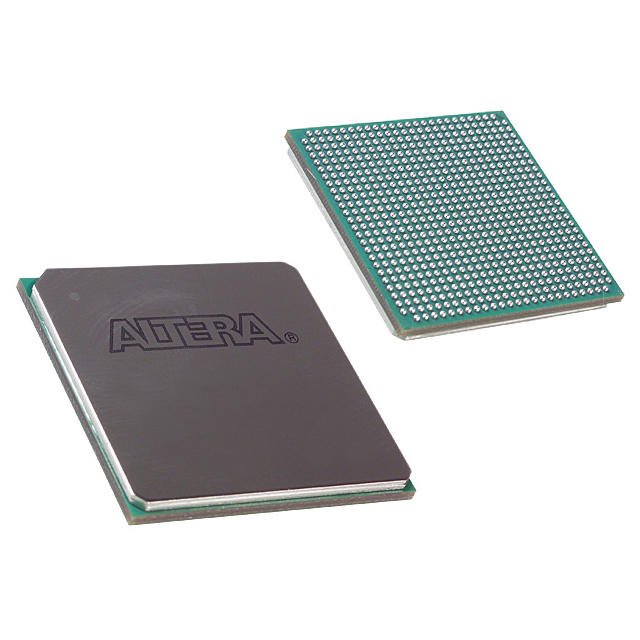
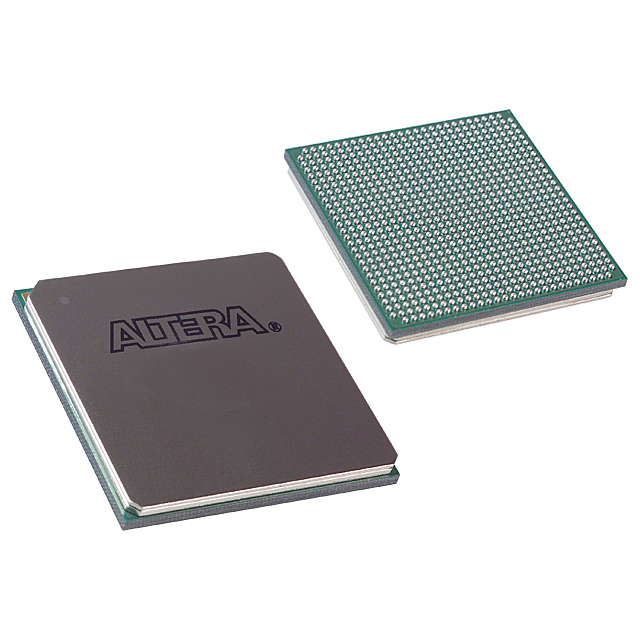
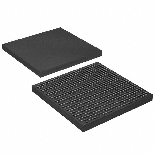
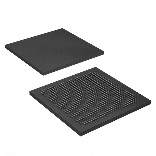
Overview of 10AX027E2F27I2SG – Arria 10 GX FPGA, 270,000 Logic Elements, 672‑BBGA
The 10AX027E2F27I2SG is an Intel Arria 10 GX field programmable gate array (FPGA) offered in a 672‑ball BGA (FCBGA) package. It is a 20‑nm mid‑range FPGA architecture designed for performance and power efficiency, suitable for applications across wireless, wireline, broadcast, computing, medical and military markets.
With 270,000 logic elements, 17,870,848 bits of embedded RAM and up to 240 I/O pins, this device targets midrange designs that require high logic density, flexible I/O and advanced on‑chip DSP and memory resources while operating over an industrial temperature range.
Key Features
- 20 nm Mid‑Range FPGA Architecture Delivers a balance of performance and power efficiency as described for the Intel Arria 10 device family.
- Logic Capacity 270,000 logic elements to implement complex midrange digital designs and custom logic blocks.
- Embedded Memory 17,870,848 total RAM bits for on‑chip buffering, packet memory and intermediate data storage.
- DSP Resources Variable‑precision DSP block architecture is included in the Arria 10 family for configurable signal processing and arithmetic acceleration.
- I/O and Package Up to 240 I/O pins in a 672‑BBGA FCBGA package (supplier package: 672‑FBGA, FC 27×27) for dense board‑level integration.
- High‑Speed Interfaces and Hard IP Family features include low‑power serial transceivers, PCIe Gen1/Gen2/Gen3 hard IP, enhanced PCS hard IP for Interlaken and 10 Gbps Ethernet support, and flexible transceiver clocking and PLL sources.
- Power and Voltage Supported core voltage supply range of 870 mV to 980 mV, reflecting the device’s low‑voltage design targets and power‑saving technologies.
- Configuration and Reliability Supports dynamic and partial reconfiguration, SEU error detection and correction capabilities, and incremental compilation workflows as part of the Arria 10 device family.
- Operating Range Industrial operating temperature range from −40 °C to 100 °C for deployment in temperature‑sensitive environments.
Typical Applications
- Wireless Infrastructure — Channel and switch cards in remote radio heads and mobile backhaul systems that require programmable signal processing and real‑time logic.
- Wireline Networking — 40G/100G muxponders, transponders and line cards where high‑speed interfaces and embedded memory support packet handling and lane aggregation.
- Broadcast and Video — Studio switching, transport and professional audio/video processing benefiting from on‑chip DSP and memory resources.
- Computing and Storage — Server acceleration, flash cache and cloud compute applications that leverage programmable logic and PCIe hard IP.
- Medical and Defense Systems — Diagnostic imaging, radar and secure communications that require industrial temperature operation and reconfigurable compute resources.
Unique Advantages
- High Logic Density: 270,000 logic elements enable implementation of complex midrange designs without external logic expansion.
- Substantial On‑Chip Memory: 17,870,848 bits of embedded RAM reduce dependence on external memory for buffering and data staging.
- Industrial Temperature Capability: −40 °C to 100 °C rating supports deployment in harsh or temperature‑variable environments.
- Flexible High‑Speed Connectivity: Integrated low‑power serial transceiver features and PCIe hard IP provide options for high‑bandwidth interfaces.
- Power‑Conscious Operation: 870–980 mV core supply range aligns with the family’s power‑saving technologies for energy‑sensitive designs.
- Reconfigurable and Reliable: Support for dynamic/partial reconfiguration, SEU detection and incremental compilation enables adaptable designs and in‑field updates.
Why Choose 10AX027E2F27I2SG?
The 10AX027E2F27I2SG Arria 10 GX FPGA combines substantial logic capacity, embedded memory, DSP capability and flexible high‑speed interfaces in a single industrial‑grade package. It is positioned for midrange applications that require a balance of performance, power efficiency and reconfigurability.
As part of the Intel Arria 10 device family, this device benefits from the family’s documented features such as clocking and PLL resources, transceiver and hard IP support, as well as available device handbooks and design recommendations to guide hardware and software development.
Request a quote or submit an RFQ for the 10AX027E2F27I2SG to check pricing and availability for your design.


Date Founded: 1968
Headquarters: Santa Clara, California, USA
Employees: 130,000+
Revenue: $54.23 Billion
Certifications and Memberships: ISO9001:2015, ISO14001:2015, ISO17025:2017, ISO27001:2022, ISO45001:2018, ISO50001:2018


