
10AX027E2F27E2SG
| Part Description |
Arria 10 GX Field Programmable Gate Array (FPGA) IC 240 17870848 270000 672-BBGA, FCBGA |
|---|---|
| Quantity | 1,220 Available (as of June 15, 2026) |

| Product Category | Field Programmable Gate Array (FPGA) |
|---|---|
| Manufacturer | Intel |
| Manufacturing Status | Active |
| Manufacturer Standard Lead Time | 16 Weeks |
| Datasheet |
Specifications & Environmental
| Device Package | 672-FBGA, FC (27x27) | Grade | Extended | Operating Temperature | 0°C – 100°C | ||
|---|---|---|---|---|---|---|---|
| Package / Case | 672-BBGA, FCBGA | Number of I/O | 240 | Voltage | 870 mV - 980 mV | ||
| Mounting Method | Surface Mount | RoHS Compliance | RoHS Compliant | REACH Compliance | REACH Unaffected | ||
| Moisture Sensitivity Level | 3 (168 Hours) | Number of LABs/CLBs | 101620 | Number of Logic Elements/Cells | 270000 | ||
| Number of Gates | N/A | ECCN | 5A002A1 | HTS Code | 8542.39.0001 | ||
| Qualification | N/A | Total RAM Bits | 17870848 |
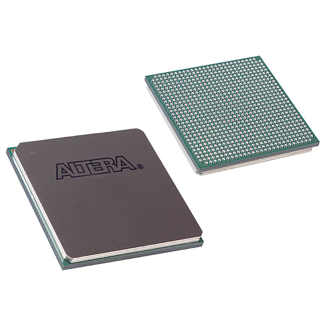
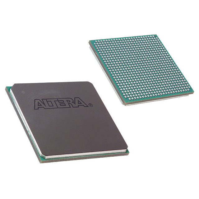
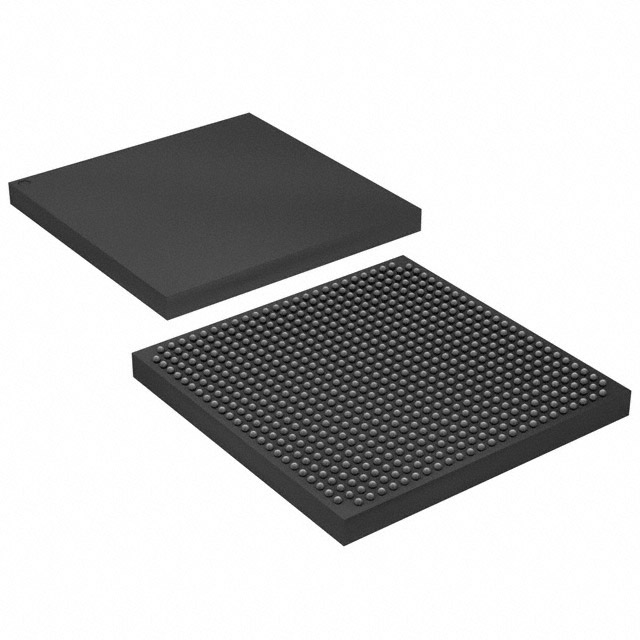
Overview of 10AX027E2F27E2SG – Arria 10 GX FPGA, 672‑BBGA, 240 I/O
The 10AX027E2F27E2SG is an Intel Arria 10 GX Field Programmable Gate Array (FPGA) in a 672‑ball BGA (FCBGA) package. It is a 20‑nm mid‑range FPGA family member designed for high‑performance, power‑sensitive applications and system integration.
With 270,000 logic elements and 17,870,848 bits of embedded RAM, this device targets markets such as wireless, wireline, broadcast, computing and storage, medical, and defense where a balance of performance and power efficiency is required.
Key Features
- Core Logic 270,000 logic elements provide substantial programmable fabric for complex digital designs.
- Embedded Memory 17,870,848 total RAM bits and embedded memory block architectures support large on‑chip buffering and data storage.
- High‑Speed I/O and Transceivers 240 I/O pins and device‑level transceiver features (as described in the Arria 10 device overview) enable high‑bandwidth external connectivity and serial links.
- DSP and Compute Blocks Variable‑precision DSP blocks (described in the device overview) facilitate signal processing and arithmetic-intensive tasks within the FPGA fabric.
- Clocking and PLLs Advanced clock networks with fractional synthesis and I/O PLL sources support flexible timing architectures and multi‑domain clocking.
- Protocol Hard IP Integrated hard IP options referenced in the device overview include PCIe Gen1/Gen2/Gen3 and enhanced PCS hard IP for high‑speed protocols such as 10 Gbps Ethernet and Interlaken.
- Package and Mounting 672‑FBGA (27×27 mm) FCBGA package, surface‑mount mounting for standard PCB assembly processes.
- Power Supply Range Core voltage supply range from 870 mV to 980 mV for core power rails.
- Operating Range and Grade Extended grade with an operating temperature range of 0 °C to 100 °C.
- Compliance RoHS‑compliant.
Typical Applications
- Wireless Infrastructure Channel and switch cards in remote radio heads and mobile backhaul equipment leveraging programmable logic and transceiver capabilities.
- Wireline Networking 40G/100G muxponders, transponders, and line cards where high‑speed serial protocols and protocol hard IP are required.
- Broadcast and Video Studio switches, transport and videoconferencing equipment that need on‑chip processing and large embedded memory for media buffering.
- Computing and Storage Acceleration Server acceleration, flash cache, and cloud computing applications using programmable compute and DSP resources.
- Medical and Defense Systems Diagnostic imaging, radar, and electronic warfare applications that benefit from configurable logic, DSP blocks, and robust clocking.
Unique Advantages
- High Logic Density: 270,000 logic elements let you implement complex algorithms and large custom accelerators on a single device.
- Substantial On‑Chip Memory: Nearly 18 Mb of embedded RAM reduces external memory dependence and improves data throughput.
- Comprehensive I/O and Protocol Support: 240 I/O and device‑level hard IP for PCIe and high‑speed Ethernet enable integration into modern communication systems.
- Power‑Efficient Mid‑Range Platform: Part of the Arria 10 family engineered for performance with power‑saving features, suitable for power‑sensitive designs.
- Package Options for Compact Systems: 672‑ball FCBGA (27×27 mm) package supports high pin‑count designs in a compact form factor.
- Extended Temperature Grade: 0 °C to 100 °C operating range supports a wide set of commercial and ruggedized deployments.
Why Choose 10AX027E2F27E2SG?
The 10AX027E2F27E2SG positions itself as a performance‑oriented, power‑conscious mid‑range FPGA with a balance of large logic capacity, extensive on‑chip memory, and broad I/O/protocol capabilities. It is well suited for engineers building wireless, wireline, broadcast, compute acceleration, medical imaging, and defense systems that require programmable flexibility along with integrated protocol support.
Backed by the Intel Arria 10 device documentation and device‑level features such as variable‑precision DSP blocks, advanced clocking, and protocol hard IP, this device offers a scalable platform for designs that must combine compute density, memory capacity, and high‑speed connectivity.
Request a quote or submit an inquiry to get pricing and availability for the 10AX027E2F27E2SG.


Date Founded: 1968
Headquarters: Santa Clara, California, USA
Employees: 130,000+
Revenue: $54.23 Billion
Certifications and Memberships: ISO9001:2015, ISO14001:2015, ISO17025:2017, ISO27001:2022, ISO45001:2018, ISO50001:2018


