
10AX048E3F29I2SG
| Part Description |
Arria 10 GX Field Programmable Gate Array (FPGA) IC 360 5664768 480000 780-BBGA, FCBGA |
|---|---|
| Quantity | 1,211 Available (as of June 15, 2026) |

| Product Category | Field Programmable Gate Array (FPGA) |
|---|---|
| Manufacturer | Intel |
| Manufacturing Status | Active |
| Manufacturer Standard Lead Time | 16 Weeks |
| Datasheet |
Specifications & Environmental
| Device Package | 780-FBGA, FC (29x29) | Grade | Industrial | Operating Temperature | -40°C – 100°C | ||
|---|---|---|---|---|---|---|---|
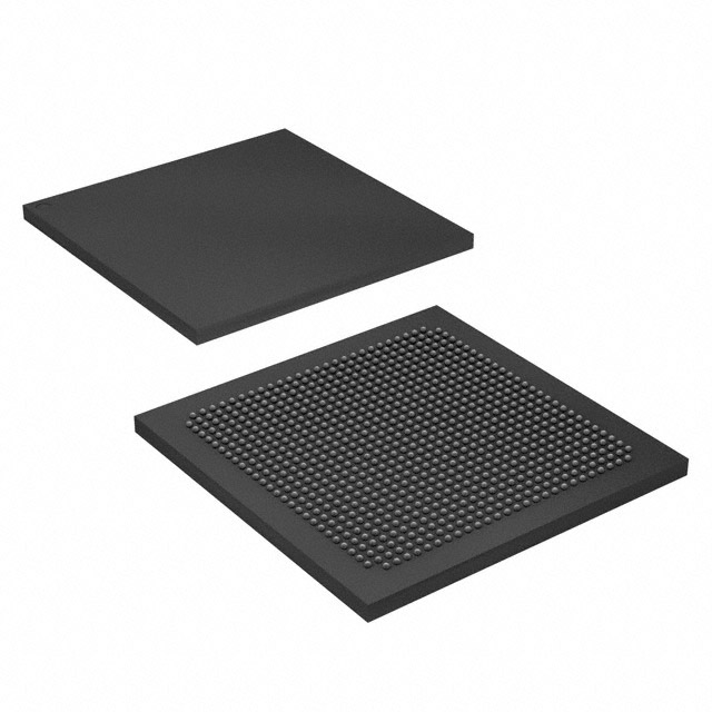
| Package / Case | 780-BBGA, FCBGA | Number of I/O | 360 | Voltage | 870 mV - 930 mV | ||
| Mounting Method | Surface Mount | RoHS Compliance | RoHS Compliant | REACH Compliance | REACH Unaffected | ||
| Moisture Sensitivity Level | 3 (168 Hours) | Number of LABs/CLBs | 183590 | Number of Logic Elements/Cells | 480000 | ||
| Number of Gates | N/A | ECCN | 5A002A1 | HTS Code | 8542.39.0001 | ||
| Qualification | N/A | Total RAM Bits | 5664768 |
Overview of 10AX048E3F29I2SG – Arria 10 GX Field Programmable Gate Array (FPGA), 480,000 logic elements, 360 I/O, 780‑BBGA
The 10AX048E3F29I2SG is an Intel Arria 10 GX field programmable gate array (FPGA) in a 780‑ball FCBGA package. It is a 20‑nm mid‑range FPGA device designed for high‑performance, power‑sensitive applications across wireless, wireline, broadcast, computing, medical and military markets.
With 480,000 logic elements, 5,664,768 bits of embedded RAM and up to 360 I/O, this device targets designs that require significant logic density, on‑chip memory and flexible high‑speed interfaces while operating across an industrial temperature range.
Key Features
- Core Density — 480,000 logic elements provide substantial programmable logic capacity for complex FPGA designs.
- Embedded Memory — 5,664,768 total RAM bits enable large on‑chip buffering and memory structures for data processing and packet handling.
- I/O and Packaging — Up to 360 general‑purpose I/O in a 780‑BBGA (29×29) surface‑mount FCBGA package suitable for compact, high‑pin‑count board designs.
- Transceivers and PHY Hard IP — Arria 10 family features include low‑power serial transceivers, enhanced PCS hard IP for Interlaken and 10 Gbps Ethernet, and support for multiple transceiver channels for high‑speed serial links.
- External Memory and PCIe — Architecture and device family support external memory interfaces and PCIe Gen1/Gen2/Gen3 hard IP for system expansion and high‑bandwidth I/O.
- Clocking and PLLs — Fractional synthesis and I/O PLLs and robust clock networks are provided for precise timing and multi‑clock domain designs.
- Configuration and Reliability — Device family supports dynamic and partial reconfiguration and SEU error detection and correction features as part of the Arria 10 architecture.
- Power and Supply — Operates from supply voltages in the 870 mV to 930 mV range and implements family power‑management features for power‑sensitive applications.
- Industrial Temperature Range — Rated for operation from −40 °C to 100 °C for deployment in industrial environments.
- RoHS Compliance — Device is RoHS compliant.
Typical Applications
- Wireless Infrastructure — Channel and switch cards in remote radio heads and mobile backhaul systems where FPGA logic density and transceiver capability are required.
- Wireline Networking — 40G/100G muxponders, transponders and line cards that leverage high‑speed PHY hard IP and programmable logic for packet processing and bridging.
- Broadcast — Studio switching and professional audio/video processing that benefit from large on‑chip memory and flexible I/O.
- Computing and Storage — Flash cache, server acceleration and cloud compute roles that need substantial logic resources and PCIe connectivity.
- Medical and Defense Systems — Diagnostic imaging, radar and secure communications applications that require high logic density and industrial temperature operation.
Unique Advantages
- High Logic Capacity: 480,000 logic elements support complex algorithms, signal processing and protocol implementations on a single device.
- Significant On‑Chip Memory: 5,664,768 bits of embedded RAM reduce external memory dependence and simplify data buffering and state storage.
- Comprehensive High‑Speed I/O: 360 I/O pins and dedicated transceiver hard IP enable multiple high‑bandwidth links and flexible board integration.
- System Integration: Arria 10 family features such as PLLs, PCIe hard IP and enhanced PCS IP accelerate system‑level integration and reduce time to market.
- Industrial Robustness: −40 °C to 100 °C operating range and surface‑mount FCBGA packaging support deployment in demanding environmental conditions.
- Power‑Aware Design: Family power‑management technologies and an 870–930 mV supply range help optimize power consumption for mid‑range, power‑sensitive applications.
Why Choose 10AX048E3F29I2SG?
The 10AX048E3F29I2SG combines the programmable capacity and memory resources required for mid‑range, high‑performance applications with the system‑level features of the Intel Arria 10 device family. Its balance of logic density, embedded RAM and high‑speed I/O makes it suitable for designs that demand substantial on‑chip processing, interface flexibility and deployment across industrial temperature conditions.
This device is well suited to engineering teams building wireless and wireline infrastructure, broadcast systems, server acceleration, medical imaging and defense electronics that rely on a documented device family and available architecture features for scalable, reliable implementations.
Request a quote or submit an inquiry to receive pricing and availability information for the 10AX048E3F29I2SG.


Date Founded: 1968
Headquarters: Santa Clara, California, USA
Employees: 130,000+
Revenue: $54.23 Billion
Certifications and Memberships: ISO9001:2015, ISO14001:2015, ISO17025:2017, ISO27001:2022, ISO45001:2018, ISO50001:2018


