
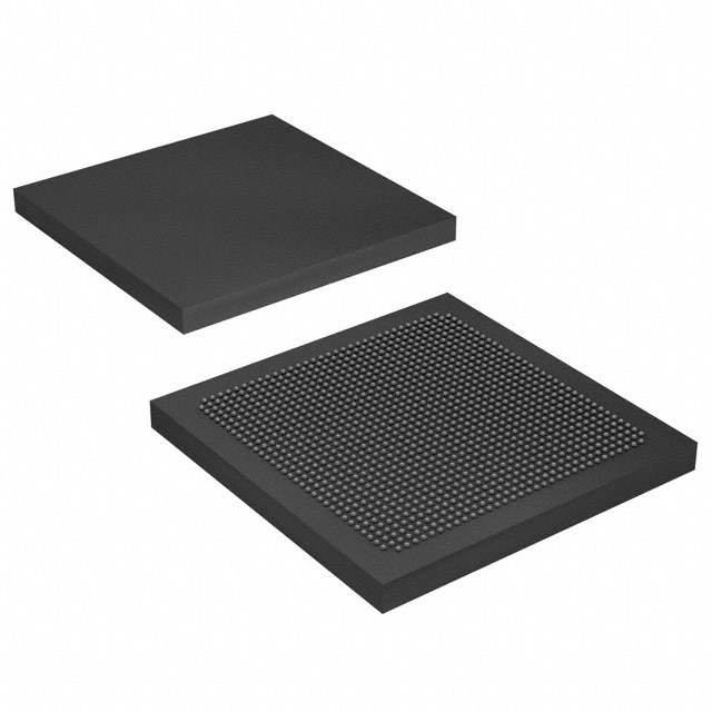
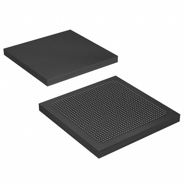
10AX066H3F34E2LG
| Part Description |
Arria 10 GX Field Programmable Gate Array (FPGA) IC 492 49610752 660000 1152-BBGA, FCBGA |
|---|---|
| Quantity | 171 Available (as of October 7, 2026) |
| Product Category | Field Programmable Gate Array (FPGA) |
|---|---|
| Manufacturer | Intel |
| Manufacturing Status | Active |
| Manufacturer Standard Lead Time | 12 Weeks |
| Datasheet |
Specifications & Environmental
| Device Package | 1152-FCBGA (35x35) | Grade | Extended | Operating Temperature | 0°C – 100°C | ||
|---|---|---|---|---|---|---|---|
| Package / Case | 1152-BBGA, FCBGA | Number of I/O | 492 | Voltage | 870 mV - 930 mV | ||
| Mounting Method | Surface Mount | RoHS Compliance | RoHS Compliant | REACH Compliance | REACH Unaffected | ||
| Moisture Sensitivity Level | 3 (168 Hours) | Number of LABs/CLBs | 250540 | Number of Logic Elements/Cells | 660000 | ||
| Number of Gates | N/A | ECCN | 3A001A7B | HTS Code | 8542.39.0001 | ||
| Qualification | N/A | Total RAM Bits | 49610752 |
Overview of 10AX066H3F34E2LG – Arria 10 GX FPGA, 1152‑FCBGA
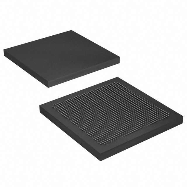
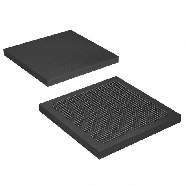
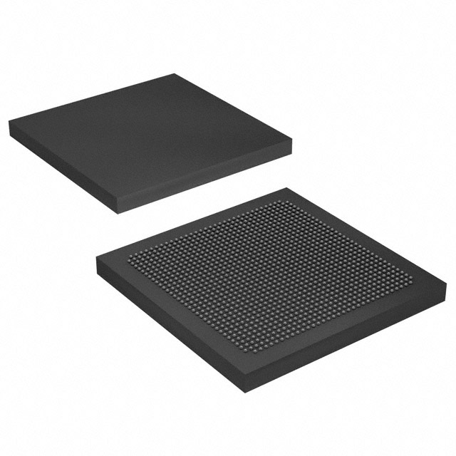
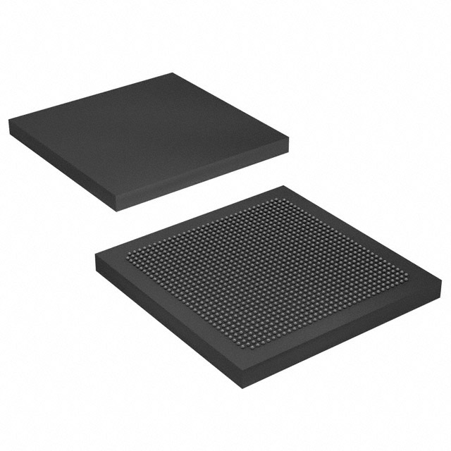
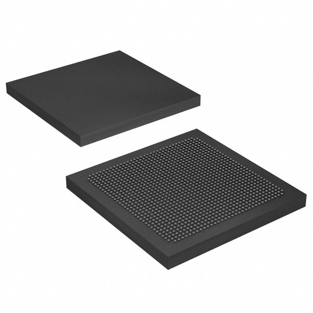
The 10AX066H3F34E2LG is an Intel Arria 10 GX field-programmable gate array (FPGA) supplied in a 1152‑FCBGA (35×35) package. It delivers a high logic capacity and substantial embedded memory in a surface-mount BGA package suited for mid-range, performance- and power-sensitive applications.
Built on the Arria 10 device family architecture, this device targets markets such as wireless, wireline, broadcast, computing and storage, medical, and military systems by combining high logic density, extensive I/O, and advanced on-chip resources for system-level integration and power efficiency.
Key Features
- Logic Capacity Provides 660,000 logic elements for implementing complex digital logic, custom accelerators, and large control/state machines.
- Embedded Memory Delivers 49,610,752 total RAM bits to support buffering, on-chip data storage, and memory-intensive algorithms.
- I/O Resources Supports 492 I/O pins to interface with high-speed peripherals, memory buses, and board-level signals.
- Package and Mounting 1152‑BBGA FCBGA package (supplier package: 1152‑FCBGA, 35×35) in a surface-mount form factor for compact PCB integration.
- Core Voltage Operates with a core supply range of 870 mV to 930 mV, matching the low-voltage requirements of modern FPGA cores.
- Operating Range and Grade Extended grade device rated for 0 °C to 100 °C operating temperature.
- Series Capabilities (Arria 10) Part of the Intel Arria 10 family—20 nm mid-range FPGAs and SoCs—offering power-efficiency technologies and architecture features such as embedded memory blocks, variable-precision DSP resources, clock networks with PLLs, and support for high-speed serial/transceiver functions as documented for the device family.
- Compliance RoHS compliant for environmental and regulatory acceptance.
Typical Applications
- Wireless Infrastructure Channel and switch cards in remote radio heads and mobile backhaul equipment where high logic density and integrated memory simplify signal processing and control functions.
- Wireline Communications Line cards, muxponders, and transponders (40G/100G) requiring extensive I/O and on-chip resources for packet processing and protocol handling.
- Broadcast and Media Studio switches and professional audio/video systems that benefit from flexible logic and large embedded memory for media stream handling and switching.
- Computing and Storage Flash cache, server acceleration, and cloud computing applications where programmable logic and DSP capabilities can be used to offload compute-intensive tasks.
- Medical and Defense Diagnostic imaging, radar, and guidance/control applications that leverage the device’s logic density and memory for real-time data processing (as described for the Arria 10 family).
Unique Advantages
- High Logic Density: 660,000 logic elements enable implementation of large, complex designs and custom accelerators on a single device.
- Large On-Chip Memory: Nearly 50 Mbits of embedded RAM reduce external memory dependence and improve system throughput for buffering and data-intensive functions.
- Extensive I/O Count: 492 I/O pins provide broad connectivity options for peripherals, memory interfaces, and board-level routing.
- Compact, Deployable Package: 1152‑FCBGA (35×35) surface-mount package supports high-density PCB layouts while maintaining robust thermal and mechanical integration.
- Power-Efficient Family Architecture: As part of the Arria 10 family (20 nm), the device benefits from documented power-saving technologies and architectural choices intended for performance-sensitive, power-conscious designs.
- Extended Operating Range: Extended-grade rating and 0 °C to 100 °C operating temperature support a wide range of commercial and industrial environments.
Why Choose 10AX066H3F34E2LG?
The 10AX066H3F34E2LG positions itself as a scalable, high-capacity FPGA option within the Intel Arria 10 GX lineup—providing the logic density, embedded memory, and I/O required for complex mid-range designs. Its package and electrical characteristics make it suitable for board-level integration where compact form factor and reliable operation across a broad temperature window are required.
Design teams focused on wireless and wireline communications, broadcast, compute acceleration, or imaging systems will find the device’s combination of resources and Arria 10 family features useful for consolidating functions, reducing external components, and enabling flexible hardware programmability over the product lifecycle.
Request a quote or submit an inquiry to receive pricing and availability information for 10AX066H3F34E2LG.





















Date Founded: 1968
Headquarters: Santa Clara, California, USA
Employees: 130,000+
Revenue: $54.23 Billion
Certifications and Memberships: ISO9001:2015, ISO14001:2015, ISO17025:2017, ISO27001:2022, ISO45001:2018, ISO50001:2018


