
10AX066H3F34E2SG
| Part Description |
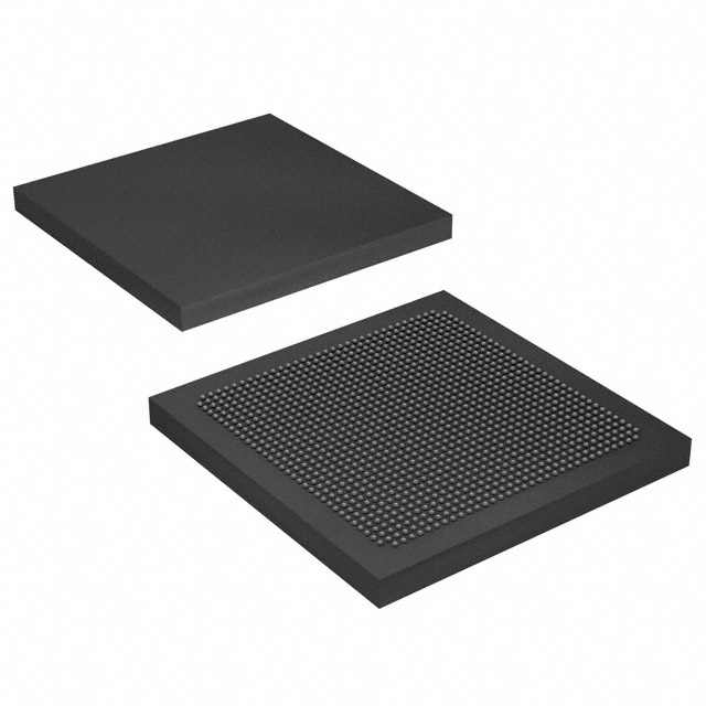
Arria 10 GX Field Programmable Gate Array (FPGA) IC 492 49610752 660000 1152-BBGA, FCBGA |
|---|---|
| Quantity | 886 Available (as of June 15, 2026) |

| Product Category | Field Programmable Gate Array (FPGA) |
|---|---|
| Manufacturer | Intel |
| Manufacturing Status | Active |
| Manufacturer Standard Lead Time | 12 Weeks |
| Datasheet |
Specifications & Environmental
| Device Package | 1152-FCBGA (35x35) | Grade | Extended | Operating Temperature | 0°C – 100°C | ||
|---|---|---|---|---|---|---|---|
| Package / Case | 1152-BBGA, FCBGA | Number of I/O | 492 | Voltage | 870 mV - 930 mV | ||
| Mounting Method | Surface Mount | RoHS Compliance | RoHS Compliant | REACH Compliance | REACH Unaffected | ||
| Moisture Sensitivity Level | 3 (168 Hours) | Number of LABs/CLBs | 250540 | Number of Logic Elements/Cells | 660000 | ||
| Number of Gates | N/A | ECCN | 3A001A7B | HTS Code | 8542.39.0001 | ||
| Qualification | N/A | Total RAM Bits | 49610752 |
Overview of 10AX066H3F34E2SG – Arria 10 GX FPGA, 1152‑FCBGA (35×35)
The 10AX066H3F34E2SG is an Intel Arria 10 GX field‑programmable gate array (FPGA) device from the Arria 10 family of 20 nm mid‑range FPGAs and SoCs. It combines high logic density and on‑chip memory with integrated high‑speed interfaces and power‑saving technologies targeted at midrange, performance‑sensitive applications.
Typical markets and applications for the Arria 10 family include wireless and wireline communications, broadcast, computing and storage, medical imaging, and military systems where performance, integration, and power efficiency are required.
Key Features
- Logic Capacity — 660,000 logic elements to implement complex digital designs and custom logic functions.
- Embedded Memory — 49,610,752 total RAM bits of on‑chip memory for buffering, packet processing, and algorithmic storage.
- I/O and Packaging — 492 user I/O pins in a 1152‑FBGA (1152‑FCBGA, 35×35) package; surface‑mount mounting type for compact board designs.
- Power and Voltage — Core voltage supply range of 870 mV to 930 mV and a family focus on power‑saving technologies to support energy‑sensitive designs.
- Temperature and Grade — Extended grade with an operating temperature range of 0 °C to 100 °C for deployment in controlled‑environment applications.
- Adaptive Logic and DSP — Family features include Adaptive Logic Modules and variable‑precision DSP blocks for arithmetic and signal processing workloads.
- High‑Speed Interfaces — Arria 10 family documentation lists PCIe Gen1/Gen2/Gen3 hard IP, enhanced PCS hard IP for Interlaken and 10 Gbps Ethernet, and low‑power serial transceivers.
- Clocking and Reconfiguration — Rich clock network architecture with PLL clock sources, plus support for dynamic and partial reconfiguration as described in the device overview.
- System Reliability — Device documentation includes SEU error detection and correction and device errata/design recommendations for robust deployment.
- Compliance — RoHS compliant.
Typical Applications
- Wireless Infrastructure — Channel and switch cards, and mobile backhaul equipment using high logic density and transceiver capabilities for RF and baseband processing.
- Wireline Networking — 40G/100G muxponders, transponders, and line cards leveraging embedded memory and hard IP for high‑speed packet and line processing.
- Broadcast and Media — Studio switches and professional video systems that benefit from large on‑chip memory and flexible I/O for video transport and switching.
- Computing and Storage Acceleration — Flash cache, server acceleration, and cloud compute offload functions using dense logic and DSP resources.
- Medical and Defense Systems — Diagnostic imaging and radar/control applications that require significant computation and configurable I/O in an extended‑grade device.
Unique Advantages
- High logic density: 660,000 logic elements provide capacity for complex algorithms, protocol stacks, and custom hardware acceleration.
- Large on‑chip memory: Nearly 49.6 million RAM bits reduce dependence on external memory for many buffering and processing tasks.
- Integrated high‑speed interfaces: Family‑level support for PCIe Gen1/2/3, 10 Gbps Ethernet, and Interlaken along with low‑power transceivers simplifies high‑bandwidth system design.
- Flexible clocking and reconfiguration: PLLs, rich clock networks, and support for dynamic/partial reconfiguration aid iterative development and in‑field updates.
- Compact system implementation: 1152‑FCBGA (35×35) package and surface‑mount mounting enable dense board layouts for space‑constrained applications.
- Extended operating range: Extended grade and 0 °C to 100 °C operation suit controlled‑environment industrial and commercial deployments.
Why Choose 10AX066H3F34E2SG?
The 10AX066H3F34E2SG delivers a balanced combination of logic capacity, embedded memory, high‑speed interfaces, and power‑conscious architecture drawn from the Intel Arria 10 device family. Its extended grade, broad feature set, and high I/O count make it a compelling choice for midrange designs requiring significant on‑chip resources and flexible connectivity.
Designed for engineers building communications, broadcast, compute‑acceleration, and imaging systems, this device benefits from Arria 10 family documentation and device‑level features that support design optimization, partial reconfiguration, and system reliability.
Request a quote or submit an inquiry to obtain pricing, lead time, and availability for the 10AX066H3F34E2SG.


Date Founded: 1968
Headquarters: Santa Clara, California, USA
Employees: 130,000+
Revenue: $54.23 Billion
Certifications and Memberships: ISO9001:2015, ISO14001:2015, ISO17025:2017, ISO27001:2022, ISO45001:2018, ISO50001:2018


