
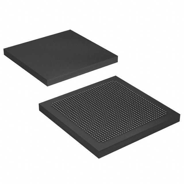
10AX066K1F35E1HG
| Part Description |
Arria 10 GX Field Programmable Gate Array (FPGA) IC 492 49610752 660000 1152-BBGA, FCBGA |
|---|---|
| Quantity | 422 Available (as of June 10, 2026) |

| Product Category | Field Programmable Gate Array (FPGA) |
|---|---|
| Manufacturer | Intel |
| Manufacturing Status | Active |
| Manufacturer Standard Lead Time | 12 Weeks |
| Datasheet |
Specifications & Environmental
| Device Package | 1152-FCBGA (35x35) | Grade | Extended | Operating Temperature | 0°C – 100°C | ||
|---|---|---|---|---|---|---|---|
| Package / Case | 1152-BBGA, FCBGA | Number of I/O | 492 | Voltage | 870 mV - 980 mV | ||
| Mounting Method | Surface Mount | RoHS Compliance | RoHS Compliant | REACH Compliance | REACH Unaffected | ||
| Moisture Sensitivity Level | 3 (168 Hours) | Number of LABs/CLBs | 250540 | Number of Logic Elements/Cells | 660000 | ||
| Number of Gates | N/A | ECCN | 5A002A1 | HTS Code | 8542.39.0001 | ||
| Qualification | N/A | Total RAM Bits | 49610752 |
Overview of 10AX066K1F35E1HG – Arria 10 GX FPGA, 1152‑FCBGA
The 10AX066K1F35E1HG is an Intel Arria 10 GX field programmable gate array (FPGA) supplied in a 1152‑FCBGA (35×35) package for surface‑mount applications. It is a member of the Arria 10 device family of 20 nm mid‑range FPGAs and SoCs designed for performance‑sensitive, power‑efficient applications.
With high logic density, substantial on‑chip RAM, broad I/O count and support for high‑speed serial connectivity and hard IP, this device targets midrange markets such as wireless, wireline, broadcast and computing applications that need integrated programmable logic and connectivity.
Key Features
- Core logic — 660,000 logic elements provide substantial programmable capacity for complex custom logic, packet processing and acceleration tasks.
- Embedded memory — 49,610,752 total RAM bits of on‑chip memory to support large buffering, caching and user memory structures without immediate external memory dependence.
- I/O and package — 492 user I/O pins in a 1152‑FCBGA (35×35) package, optimized for dense board integration and high‑pin‑count designs. Mounting type: surface mount.
- Power and thermal — Core voltage supply range of 870 mV to 980 mV and an operating temperature range of 0 °C to 100 °C; device is specified as Extended grade.
- High‑speed connectivity and hard IP — Includes low‑power serial transceivers and hard IP such as PCIe Gen1/2/3 and enhanced PCS support referenced for 10 Gbps Ethernet and Interlaken applications.
- Processing and DSP — Device family supports variable‑precision DSP blocks and SoC integration options such as a Hard Processor System, enabling mixed compute and FPGA workflows.
- Configuration and reliability — Supports dynamic and partial reconfiguration, SEU error detection and correction mechanisms, plus documented power management and incremental compilation strategies.
- Standards and compliance — RoHS compliant.
Typical Applications
- Wireless infrastructure — Channel cards and switch cards in remote radio heads and mobile backhaul equipment leveraging dense logic and high‑speed serial links.
- Wireline and transport — 40G/100G muxponders, transponders and line cards where integrated connectivity IP and programmable logic accelerate packet processing and protocol bridging.
- Broadcast and media — Studio switches, video transport and professional audio/video systems that require deterministic logic, on‑chip memory and high I/O density.
- Computing and storage — Server acceleration, flash cache and cloud compute offload tasks benefiting from large on‑chip RAM and flexible DSP resources.
- Medical and imaging — Diagnostic imaging and scanner processing that use programmable logic for custom signal processing and data aggregation.
Unique Advantages
- High logic density: 660,000 logic elements enable large, integrated FPGA designs without immediate partitioning across multiple devices.
- Significant on‑chip memory: Nearly 50 Mbit of RAM supports large buffers and data structures directly on the FPGA fabric, reducing external memory bandwidth needs.
- Comprehensive I/O and package: 492 user I/Os in a 1152‑FCBGA allow dense connectivity and flexible board routing for complex systems.
- Integrated connectivity IP: Built‑in support for PCIe Gen1/2/3 and high‑speed serial transceivers simplifies implementation of high‑throughput link interfaces.
- Power‑aware architecture: Family‑level power‑saving technologies combined with a defined core voltage range support designs with power efficiency goals.
- Extended operating range: Extended grade with 0 °C to 100 °C operating range supports deployment in a wide set of commercial and industrial environments.
Why Choose 10AX066K1F35E1HG?
This Arria 10 GX device balances high programmable capacity, sizable on‑chip memory and comprehensive connectivity IP in a surface‑mount 1152‑FCBGA package. It is positioned for midrange applications that require a combination of logic density, integrated high‑speed I/O and power‑sensitive operation.
For engineering teams building wireless infrastructure, high‑speed transport, media processing or compute acceleration systems, the 10AX066K1F35E1HG provides a scalable, Intel Arria 10 family‑based solution with features for on‑chip signal processing, robust connectivity and configuration flexibility.
Request a quote or submit a quotation request for part number 10AX066K1F35E1HG to evaluate this Arria 10 GX FPGA for your next design.


Date Founded: 1968
Headquarters: Santa Clara, California, USA
Employees: 130,000+
Revenue: $54.23 Billion
Certifications and Memberships: ISO9001:2015, ISO14001:2015, ISO17025:2017, ISO27001:2022, ISO45001:2018, ISO50001:2018


