
10AX090N2F45I2SG
| Part Description |
Arria 10 GX Field Programmable Gate Array (FPGA) IC 768 59234304 900000 1932-BBGA, FCBGA |
|---|---|
| Quantity | 1,306 Available (as of June 14, 2026) |

| Product Category | Field Programmable Gate Array (FPGA) |
|---|---|
| Manufacturer | Intel |
| Manufacturing Status | Active |
| Manufacturer Standard Lead Time | 16 Weeks |
| Datasheet |
Specifications & Environmental
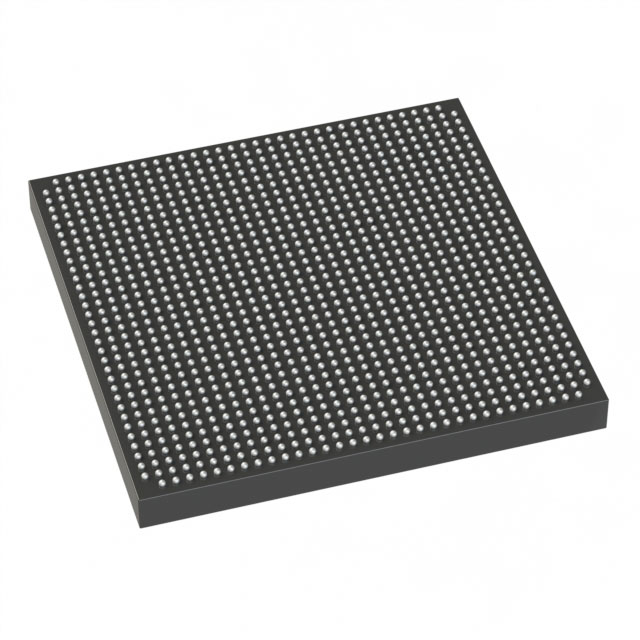
| Device Package | 1932-FCBGA (45x45) | Grade | Industrial | Operating Temperature | -40°C – 100°C | ||
|---|---|---|---|---|---|---|---|
| Package / Case | 1932-BBGA, FCBGA | Number of I/O | 768 | Voltage | 870 mV - 980 mV | ||
| Mounting Method | Surface Mount | RoHS Compliance | RoHS Compliant | REACH Compliance | REACH Unaffected | ||
| Moisture Sensitivity Level | 3 (168 Hours) | Number of LABs/CLBs | 339620 | Number of Logic Elements/Cells | 900000 | ||
| Number of Gates | N/A | ECCN | 3A001A7A | HTS Code | 8542.39.0001 | ||
| Qualification | N/A | Total RAM Bits | 59234304 |
Overview of 10AX090N2F45I2SG – Arria 10 GX FPGA, 1932-FCBGA (45×45)
The 10AX090N2F45I2SG is an Intel Arria 10 GX field programmable gate array (FPGA) device in a 1932-FCBGA (45×45) surface-mount package. It is part of the Arria 10 device family of 20 nm mid‑range FPGAs and SoCs, designed for performance and power-efficient programmable logic integration.
Targeted markets include wireless, wireline, broadcast, computing and storage, medical, and military applications where a combination of high logic density, on‑chip memory and high‑speed I/O enable packet processing, protocol bridging, signal processing and system acceleration.
Key Features
- Core logic Approximately 900,000 logic elements provide substantial programmable logic capacity for complex digital designs.
- Embedded memory 59,234,304 total RAM bits of on‑chip memory for buffering, packet storage and large data structures.
- I/O and high‑speed interfaces 768 I/O signals support high‑pin‑count connectivity. The Arria 10 family description includes hard IP for PCIe Gen1/Gen2/Gen3 and support for 10 Gbps Ethernet and Interlaken, as well as low‑power serial transceivers.
- DSP and processing Variable‑precision DSP blocks and support for a SoC Hard Processor System (HPS) are described for computation and system integration in the device family.
- Configuration and reliability The device family supports dynamic and partial reconfiguration, SEU error detection and correction, and enhanced configuration options for flexible deployment and runtime updates.
- Package, mounting and grade Surface‑mount 1932‑FCBGA package (1932‑BBGA notation present) in a 45×45 format; specified as Industrial grade.
- Power and thermal Supply voltage range 0.870 V to 0.980 V and operating temperature range −40 °C to 100 °C, enabling use across a wide set of industrial environments.
Typical Applications
- Wireless infrastructure Channel and switch cards in remote radio heads and mobile backhaul systems that require dense logic and high‑speed transceivers.
- Wireline communications 40G/100G muxponder and transponder line cards, line aggregation and bridging applications leveraging embedded memory and high‑speed serial interfaces.
- Broadcast and professional video Studio switching, transport and videoconferencing systems that require large on‑chip buffering and flexible protocol handling.
- Computing and storage Server acceleration, flash cache and cloud compute offload tasks using the device’s DSP resources and programmable fabric.
- Medical and defense electronics Diagnostic imaging, radar and secure communications where industrial temperature operation and reliable reconfiguration are important.
Unique Advantages
- High logic density: The ~900,000 logic elements reduce the need for multi‑device solutions and simplify board-level integration.
- Large on‑chip memory: Over 59 million RAM bits support deep buffering, packet processing and storage for streaming applications.
- Extensive I/O and connectivity: 768 I/O pins combined with documented hard IP for PCIe and 10 Gbps Ethernet speeds accelerate system-level integration.
- Industrial readiness: Specified operating range from −40 °C to 100 °C and surface‑mount 1932‑FCBGA packaging for deployed industrial systems.
- Flexible configuration and reliability: Dynamic and partial reconfiguration plus SEU detection and correction enable in‑field updates and improved uptime.
- Power‑efficient architecture: The Arria 10 family emphasizes power‑saving technologies; the device’s nominal supply range (0.870–0.980 V) supports optimized power design.
Why Choose 10AX090N2F45I2SG?
As a member of the Intel Arria 10 family, the 10AX090N2F45I2SG combines high programmable logic capacity, substantial on‑chip memory and extensive I/O to address mid‑range, performance‑sensitive applications. Its feature set is tailored for designers who need a balance of compute, memory and connectivity in a single, industrial‑rated FPGA package.
This device is appropriate for engineering teams building advanced communications, video, compute acceleration and industrial systems that require scalable performance, flexible reconfiguration and a broad set of platform features from the Arria 10 device family.
Request a quote or submit an inquiry to check availability, pricing and lead times for the 10AX090N2F45I2SG. Our team can provide the purchasing information and support you need to move forward with your design.


Date Founded: 1968
Headquarters: Santa Clara, California, USA
Employees: 130,000+
Revenue: $54.23 Billion
Certifications and Memberships: ISO9001:2015, ISO14001:2015, ISO17025:2017, ISO27001:2022, ISO45001:2018, ISO50001:2018


