
10AX090R3F40I2SG
| Part Description |
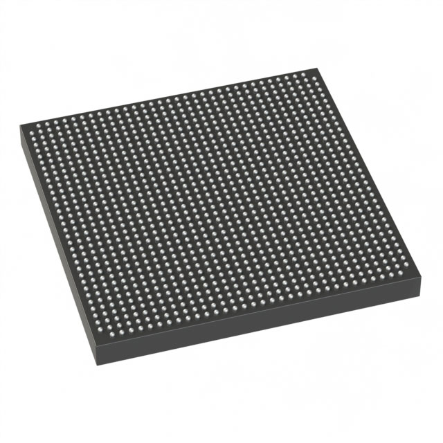
Arria 10 GX Field Programmable Gate Array (FPGA) IC 342 59234304 900000 1517-BBGA, FCBGA |
|---|---|
| Quantity | 247 Available (as of June 15, 2026) |

| Product Category | Field Programmable Gate Array (FPGA) |
|---|---|
| Manufacturer | Intel |
| Manufacturing Status | Active |
| Manufacturer Standard Lead Time | 9 Weeks |
| Datasheet |
Specifications & Environmental
| Device Package | 1517-FCBGA (40x40) | Grade | Industrial | Operating Temperature | -40°C – 100°C | ||
|---|---|---|---|---|---|---|---|
| Package / Case | 1517-BBGA, FCBGA | Number of I/O | 342 | Voltage | 870 mV - 930 mV | ||
| Mounting Method | Surface Mount | RoHS Compliance | RoHS Compliant | REACH Compliance | REACH Unaffected | ||
| Moisture Sensitivity Level | 3 (168 Hours) | Number of LABs/CLBs | 339620 | Number of Logic Elements/Cells | 900000 | ||
| Number of Gates | N/A | ECCN | 3A001A7A | HTS Code | 8542.39.0001 | ||
| Qualification | N/A | Total RAM Bits | 59234304 |
Overview of 10AX090R3F40I2SG – Arria 10 GX FPGA, 900,000 Logic Elements, 1517‑FCBGA
The 10AX090R3F40I2SG is an Intel Arria 10 GX field‑programmable gate array (FPGA) provided in a 1517‑FCBGA / 1517‑BBGA package. It is a midrange, high‑performance 20‑nm FPGA family device designed for applications that require high logic density, extensive embedded memory, and flexible I/O.
Target use cases include wireless and wireline communications, broadcast and media transport, computing and storage acceleration, and other industrial applications where performance, integration and power efficiency are important design considerations.
Key Features
- Logic Capacity 900,000 logic elements provide extensive programmable logic resources for complex FPGA designs.
- Embedded Memory 59,234,304 total RAM bits for large on‑chip buffering, packet processing, or data staging.
- I/O Resources 342 I/Os support dense external interfacing and high‑pin‑count connectivity options.
- Transceiver and IP Support Family features include low‑power serial transceivers and hard IP options such as PCIe Gen1–Gen3 and enhanced PCS hard IP for high‑speed protocols referenced in the device overview.
- DSP and Compute Blocks Variable‑precision DSP blocks are included in the Arria 10 family for compute‑intensive signal processing tasks.
- Configuration and Reconfiguration The device family supports dynamic and partial reconfiguration features as described in the device overview for flexible, in‑field design updates.
- Package & Mounting Supplied in a 1517‑FCBGA (40×40) FCBGA / 1517‑BBGA package and intended for surface‑mount assembly.
- Power and Temperature Voltage supply range 870 mV to 930 mV and industrial operating temperature range from −40 °C to 100 °C.
- Compliance RoHS‑compliant for environmental regulatory requirements.
Typical Applications
- Wireless Infrastructure Channel and switch cards in remote radio heads and mobile backhaul systems leveraging high logic density and DSP resources.
- Wireline Optical and Packet Transport 40G/100G muxponders, transponders, line cards and aggregation/bridging solutions using on‑chip memory and high‑speed serial interfaces.
- Broadcast and Professional AV Studio switches, video processing and transport applications that require deterministic I/O and large on‑chip buffering.
- Computing and Storage Acceleration Cloud server acceleration and flash cache applications where programmable logic and embedded RAM are used for low‑latency data paths.
Unique Advantages
- High programmable density: 900,000 logic elements enable consolidation of complex functions into a single FPGA, reducing board‑level component count.
- Large on‑chip memory: Nearly 59.3 Mbits of embedded RAM supports large buffers, frame storage, and packet processing without relying solely on external memory.
- Extensive I/O count: 342 I/Os accommodate multiple parallel interfaces and high‑pin‑count connectivity for flexible system integration.
- Industrial temperature range: Rated from −40 °C to 100 °C, supporting deployment in a wide range of environmental conditions.
- Power‑aware operation: The Arria 10 family emphasizes power efficiency and supports low‑voltage supply operation (870–930 mV) for optimized system power profiles.
- Robust packaging for surface mount: 1517‑FCBGA (40×40) packaging provides a compact form factor for high‑density PCB layouts.
Why Choose 10AX090R3F40I2SG?
The 10AX090R3F40I2SG positions itself as a high‑capacity, power‑efficient midrange FPGA suitable for demanding communications, broadcast, and compute acceleration designs. With 900,000 logic elements, substantial on‑chip RAM, and a broad set of family features for transceivers and IP, it enables system architects to implement complex, high‑bandwidth functions while managing board‑level complexity.
Engineers designing for industrial environments will benefit from the device’s industrial temperature rating, RoHS compliance, and surface‑mount packaging. The combination of logic density, memory capacity, I/O resources, and family feature set offers scalable integration for long‑lifecycle projects and evolving system requirements.
Request a quote or submit a sales inquiry to evaluate 10AX090R3F40I2SG for your next design and obtain pricing, availability, and ordering information.


Date Founded: 1968
Headquarters: Santa Clara, California, USA
Employees: 130,000+
Revenue: $54.23 Billion
Certifications and Memberships: ISO9001:2015, ISO14001:2015, ISO17025:2017, ISO27001:2022, ISO45001:2018, ISO50001:2018


