
10AX090R2F40I2SG
| Part Description |
Arria 10 GX Field Programmable Gate Array (FPGA) IC 342 59234304 900000 1517-BBGA, FCBGA |
|---|---|
| Quantity | 456 Available (as of June 10, 2026) |

| Product Category | Field Programmable Gate Array (FPGA) |
|---|---|
| Manufacturer | Intel |
| Manufacturing Status | Active |
| Manufacturer Standard Lead Time | 9 Weeks |
| Datasheet |
Specifications & Environmental
| Device Package | 1517-FCBGA (40x40) | Grade | Industrial | Operating Temperature | -40°C – 100°C | ||
|---|---|---|---|---|---|---|---|
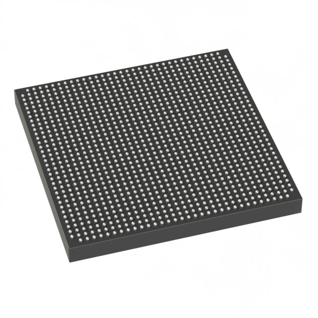
| Package / Case | 1517-BBGA, FCBGA | Number of I/O | 342 | Voltage | 870 mV - 980 mV | ||
| Mounting Method | Surface Mount | RoHS Compliance | RoHS Compliant | REACH Compliance | REACH Unaffected | ||
| Moisture Sensitivity Level | 3 (168 Hours) | Number of LABs/CLBs | 339620 | Number of Logic Elements/Cells | 900000 | ||
| Number of Gates | N/A | ECCN | 3A001A7A | HTS Code | 8542.39.0001 | ||
| Qualification | N/A | Total RAM Bits | 59234304 |
Overview of 10AX090R2F40I2SG – Arria 10 GX Field Programmable Gate Array (FPGA)
The 10AX090R2F40I2SG is an Intel Arria 10 GX FPGA offered in a 1517-FCBGA (40×40) surface-mount package. This industrial-grade device combines a large logic capacity with extensive embedded memory and I/O to address performance-sensitive, midrange FPGA applications.
Designed as part of the Arria 10 family of 20 nm mid-range FPGAs, the device targets markets that require high logic density, significant on-chip RAM, and broad I/O support while operating across a wide industrial temperature and voltage window.
Key Features
- High Logic Capacity 900,000 logic elements provide substantial programmable fabric for complex digital designs.
- Embedded Memory 59,234,304 total RAM bits of on-chip memory support large buffering, caching, and data-path implementations.
- Extensive I/O 342 I/O pins enable wide parallel interfaces and flexible board-level connectivity.
- Package and Mounting 1517-FCBGA (40×40) package in a surface-mount form factor suits dense PCB layouts and system integration.
- Industrial Operating Range Rated for -40°C to 100°C to meet industrial thermal requirements.
- Core Supply Voltage Operates from 870 mV to 980 mV, aligning with modern low-voltage FPGA core domains.
- Device Family Capabilities As part of the Arria 10 family, the device leverages 20 nm architecture and family features such as embedded memory blocks, DSP resources, and advanced clocking and configuration options documented in the Arria 10 device overview.
- RoHS Compliant Meets RoHS environmental requirements for lead-free manufacturing.
Typical Applications
- Wireless Infrastructure Channel processing and backhaul functions that benefit from the device's high logic density and large embedded RAM.
- Wireline Communications Line cards, muxponders, and transponder interfaces leveraging extensive I/O and on-chip memory for packet and signal processing.
- Broadcast and Media Studio switching, video transport and conferencing systems that require flexible logic and substantial buffering on-chip.
- Computing and Storage Acceleration Server acceleration and cache-related tasks that exploit the device's logic capacity and embedded RAM.
Unique Advantages
- Large, Programmable Fabric: 900,000 logic elements give designers the headroom to implement complex control, processing, and FPGA-accelerated functions on a single device.
- Significant On-Chip Memory: 59.2M total RAM bits reduce dependence on external memory for many buffering and caching needs, simplifying BOM and board design.
- Broad I/O Count: 342 I/Os provide flexibility for wide parallel buses, high-density connectors, and mixed-signal interface requirements.
- Industrial Reliability: Industrial-grade temperature range (-40°C to 100°C) supports deployment in demanding environments.
- Compact, Surface-Mount Packaging: The 1517-FCBGA (40×40) package enables high-density PCB integration while maintaining thermal and electrical performance.
- Documented Platform Features: As an Arria 10 family device, it benefits from published device documentation covering embedded memory types, clock networks, configuration options, and power management.
Why Choose 10AX090R2F40I2SG?
The 10AX090R2F40I2SG positions itself for designs that require substantial programmable logic, large on-chip memory, and a high I/O count within an industrial temperature envelope. Its Arria 10 family lineage provides access to documented architectural features—such as embedded memory blocks, advanced clocking, and power-management capabilities—that help accelerate development and system integration.
This device is suited to engineers and system designers building midrange, performance-sensitive applications across communications, broadcast, and compute-acceleration markets who need a scalable, well-documented FPGA platform with robust on-chip resources.
Request a quote or submit an inquiry to check pricing and availability for 10AX090R2F40I2SG and to discuss how this Arria 10 GX FPGA can meet your project requirements.


Date Founded: 1968
Headquarters: Santa Clara, California, USA
Employees: 130,000+
Revenue: $54.23 Billion
Certifications and Memberships: ISO9001:2015, ISO14001:2015, ISO17025:2017, ISO27001:2022, ISO45001:2018, ISO50001:2018


