
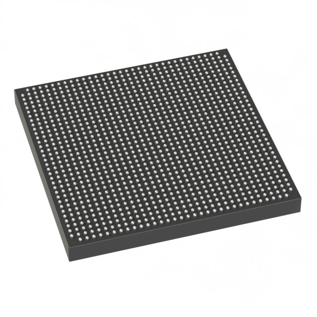
10AX090R2F40I2LG
| Part Description |
Arria 10 GX Field Programmable Gate Array (FPGA) IC 342 59234304 900000 1517-BBGA, FCBGA |
|---|---|
| Quantity | 1,384 Available (as of June 15, 2026) |

| Product Category | Field Programmable Gate Array (FPGA) |
|---|---|
| Manufacturer | Intel |
| Manufacturing Status | Active |
| Manufacturer Standard Lead Time | 9 Weeks |
| Datasheet |
Specifications & Environmental
| Device Package | 1517-FCBGA (40x40) | Grade | Industrial | Operating Temperature | -40°C – 100°C | ||
|---|---|---|---|---|---|---|---|
| Package / Case | 1517-BBGA, FCBGA | Number of I/O | 342 | Voltage | 870 mV - 980 mV | ||
| Mounting Method | Surface Mount | RoHS Compliance | RoHS Compliant | REACH Compliance | REACH Unaffected | ||
| Moisture Sensitivity Level | 3 (168 Hours) | Number of LABs/CLBs | 339620 | Number of Logic Elements/Cells | 900000 | ||
| Number of Gates | N/A | ECCN | 3A001A7A | HTS Code | 8542.39.0001 | ||
| Qualification | N/A | Total RAM Bits | 59234304 |
Overview of 10AX090R2F40I2LG – Arria 10 GX FPGA, 900,000 logic elements, 1517-FCBGA
The 10AX090R2F40I2LG is an Intel Arria 10 GX Field Programmable Gate Array (FPGA) device from the Arria 10 family of 20 nm mid-range FPGAs and SoCs. This device combines high logic density, large embedded RAM, and a broad I/O set in a 1517-FCBGA (40×40) package suitable for surface-mount applications.
Targeted at mid-range, performance-sensitive systems, the part addresses markets such as wireless, wireline, broadcast, computing and storage, medical, and defense by delivering reconfigurable logic, embedded memory, transceiver capability, and system-level features for power and configuration management.
Key Features
- High Logic Density — 900,000 logic elements for implementing complex digital logic, state machines, and custom accelerators.
- Large Embedded Memory — 59,234,304 total RAM bits to support large buffering, caching, and on-chip data structures.
- Extensive I/O — 342 I/O pins to interface with wide external memory buses, high-speed serdes, and diverse peripheral devices.
- Package and Mounting — 1517-FCBGA (40×40) package, surface-mount mounting type for standard PCB assembly processes.
- Voltage and Temperature — Core voltage supply range 870 mV to 980 mV and operating temperature range −40 °C to 100 °C (industrial grade) for a wide set of environmental conditions.
- Transceivers and High-Speed I/O — Includes capabilities described in the Arria 10 GX family such as low-power serial transceivers and multi‑Gbps channel support for high-speed links.
- Hard IP and Interfaces — Family-level support for PCIe Gen1/Gen2/Gen3 hard IP, enhanced PCS hard IP for Interlaken and 10 Gbps Ethernet, and external memory interfaces as described for Arria 10 devices.
- Programmability and Reconfiguration — Supports dynamic and partial reconfiguration features found in the Arria 10 family for flexible in-field updates and runtime adaptation.
- Power and System Features — Includes Arria 10 family power-management and clocking features such as PLLs and fractional synthesis to support optimized power and timing architectures.
- Regulatory — RoHS compliant.
Typical Applications
- Wireless Infrastructure — Channel processing, remote radio head interfaces, and mobile backhaul where reconfigurable logic and embedded memory support signal processing workloads.
- Wireline and Telecom — Line cards, muxponders, and aggregation equipment leveraging the device’s high logic density, high-speed transceivers, and PCIe/10 Gbps Ethernet hard IP capabilities.
- Broadcast and Pro AV — Video processing, studio switching, and transport applications that require large on-chip memory and abundant I/O for format conversion and routing.
- Compute and Storage Acceleration — Flash cache, cloud server acceleration, and custom compute offload where on-chip RAM and dense logic implement buffering and acceleration functions.
Unique Advantages
- Highly integrated logic and memory: 900,000 logic elements and 59,234,304 RAM bits provide the capacity to consolidate multiple functions on a single device, reducing board-level complexity.
- Robust I/O and packaging: 342 I/O pins in a 1517-FCBGA (40×40) package enable wide external interfaces and dense board routing for complex systems.
- Industrial temperature range: Rated for −40 °C to 100 °C operation, enabling deployment in temperature-challenging environments.
- Flexible system integration: Arria 10 family features such as PCIe hard IP, high-speed serial transceivers, and clocking resources simplify integration with high-speed networks and external memory.
- Reconfigurability for lifecycle flexibility: Support for dynamic and partial reconfiguration allows in-field updates and function changes without full device reprogramming.
- Low-voltage core operation: Core supply range of 870 mV to 980 mV supports modern low-voltage system architectures.
Why Choose 10AX090R2F40I2LG?
The 10AX090R2F40I2LG Arria 10 GX FPGA combines high logic capacity, extensive embedded RAM, and a comprehensive set of system-level features from the Arria 10 family to address mid-range, performance-sensitive designs. Its industrial temperature rating and broad I/O count make it suitable for demanding communications, broadcast, storage, and compute-acceleration applications.
Backed by Intel Arria 10 device documentation and family-level capabilities—such as advanced clocking, power management, transceivers, and hard IP for common interfaces—this device is positioned for designs that require scalability, reconfigurability, and integration into complex systems.
Request a quote or submit an inquiry to receive pricing and availability for the 10AX090R2F40I2LG.


Date Founded: 1968
Headquarters: Santa Clara, California, USA
Employees: 130,000+
Revenue: $54.23 Billion
Certifications and Memberships: ISO9001:2015, ISO14001:2015, ISO17025:2017, ISO27001:2022, ISO45001:2018, ISO50001:2018


