
5AGXBA1D4F31C4N
| Part Description |
Arria V GX Field Programmable Gate Array (FPGA) IC 416 8666112 75000 896-BBGA, FCBGA |
|---|---|
| Quantity | 755 Available (as of June 15, 2026) |

| Product Category | Field Programmable Gate Array (FPGA) |
|---|---|
| Manufacturer | Intel |
| Manufacturing Status | Obsolete |
| Manufacturer Standard Lead Time | Contact Us |
| Datasheet |
Specifications & Environmental
| Device Package | 896-FBGA (31x31) | Grade | Commercial | Operating Temperature | 0°C – 85°C | ||
|---|---|---|---|---|---|---|---|
| Package / Case | 896-BBGA, FCBGA | Number of I/O | 416 | Voltage | 1.07 V - 1.13 V | ||
| Mounting Method | Surface Mount | RoHS Compliance | RoHS Compliant | REACH Compliance | REACH Unknown | ||
| Moisture Sensitivity Level | 3 (168 Hours) | Number of LABs/CLBs | 3537 | Number of Logic Elements/Cells | 75000 | ||
| Number of Gates | N/A | ECCN | 3A001A2C | HTS Code | 8542.39.0001 | ||
| Qualification | N/A | Total RAM Bits | 8666112 |
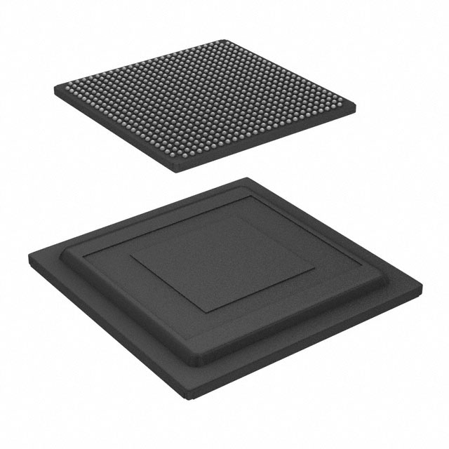
Overview of 5AGXBA1D4F31C4N – Arria V GX FPGA, 75,000 logic elements, 416 I/O
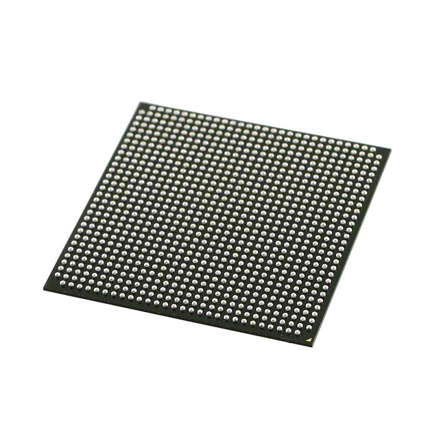
The 5AGXBA1D4F31C4N is an Intel Arria V GX field-programmable gate array supplied in a 896-ball FCBGA package. It provides a high-density programmable fabric with substantial on-chip RAM and a large number of user I/O for integration into complex digital systems.
Designed for commercial-grade applications, this device targets system designers who need a combination of logic capacity, embedded memory, and high I/O count in a surface-mount 31×31 FBGA footprint. Key value propositions include high logic density, sizeable RAM resources, and predictable operating parameters tied to its specified core voltage and temperature range.
Key Features
- Core Capacity Approx. 75,000 logic elements and 3,537 logic array blocks, providing substantial programmable logic density for complex designs.
- On-chip Memory Total RAM capacity of 8,666,112 bits to support buffering, state storage, and local data processing.
- I/O Resources Up to 416 user I/O pins to support wide parallel interfaces and diverse peripheral connections.
- Package & Mounting 896-ball FCBGA (896-BBGA / 896-FBGA, 31×31) surface-mount package for compact board integration.
- Power Specified core supply voltage range of 1.07 V to 1.13 V for defined power and timing behavior.
- Operating Conditions Commercial-grade device rated for 0 °C to 85 °C ambient operation.
- Compliance RoHS compliant for environmental and assembly considerations.
- Supporting Documentation Arria V device datasheet coverage includes electrical characteristics, switching characteristics, configuration specifications, and I/O timing (see manufacturer datasheet for full technical details).
Typical Applications
- Programmable system integration Use the device to consolidate custom logic, glue logic, and peripheral interfaces into a single programmable component, leveraging its 75,000 logic elements and 416 I/Os.
- On-board processing and buffering The 8,666,112 bits of on-chip RAM enable local data buffering, packet processing, and temporary storage for real-time algorithms.
- Prototyping and development A high-density FPGA package in a compact 31×31 FBGA footprint supports rapid iteration of digital designs and system verification at commercial temperatures.
Unique Advantages
- High integration density: Consolidate larger portions of a system into programmable logic with approximately 75,000 logic elements and thousands of logic array blocks.
- Substantial on-chip memory: 8,666,112 bits of RAM reduce external memory dependence and simplify board-level routing for many designs.
- Large I/O complement: 416 user I/Os allow flexible interfacing to processors, sensors, converters, and parallel buses without extensive external multiplexing.
- Compact package: 896-ball FCBGA (31×31) enables a small PCB footprint while maintaining high pin count for system-dense designs.
- Deterministic power window: Narrow core voltage range (1.07 V–1.13 V) helps maintain consistent timing and power planning across deployments.
- Commercial-grade reliability: Rated for 0 °C to 85 °C operation and RoHS compliant for standard commercial production environments.
Why Choose 5AGXBA1D4F31C4N?
The 5AGXBA1D4F31C4N Arria V GX FPGA delivers a balanced combination of logic density, embedded RAM, and a high I/O count in a compact 896-ball FCBGA package. Its defined core voltage window and commercial operating temperature make it suitable for designers seeking predictable electrical behavior and solid integration into commercial electronic systems.
This device is well suited for teams developing complex programmable logic solutions that require on-chip memory, wide I/O connectivity, and a high count of logic elements—providing a scalable, supported platform for medium- to high-complexity digital designs.
Request a quote or submit a purchase inquiry to receive pricing, lead-time, and availability information for the 5AGXBA1D4F31C4N Arria V GX FPGA. Our team can assist with volume requirements and delivery options.


Date Founded: 1968
Headquarters: Santa Clara, California, USA
Employees: 130,000+
Revenue: $54.23 Billion
Certifications and Memberships: ISO9001:2015, ISO14001:2015, ISO17025:2017, ISO27001:2022, ISO45001:2018, ISO50001:2018


