
5AGXBA5D4F31I5N
| Part Description |
Arria V GX Field Programmable Gate Array (FPGA) IC 384 13284352 190000 896-BBGA, FCBGA |
|---|---|
| Quantity | 412 Available (as of June 15, 2026) |

| Product Category | Field Programmable Gate Array (FPGA) |
|---|---|
| Manufacturer | Intel |
| Manufacturing Status | Obsolete |
| Manufacturer Standard Lead Time | Contact Us |
| Datasheet |
Specifications & Environmental
| Device Package | 896-FBGA (31x31) | Grade | Industrial | Operating Temperature | -40°C – 100°C | ||
|---|---|---|---|---|---|---|---|
| Package / Case | 896-BBGA, FCBGA | Number of I/O | 384 | Voltage | 1.07 V - 1.13 V | ||
| Mounting Method | Surface Mount | RoHS Compliance | RoHS Compliant | REACH Compliance | REACH Unknown | ||
| Moisture Sensitivity Level | 3 (168 Hours) | Number of LABs/CLBs | 8962 | Number of Logic Elements/Cells | 190000 | ||
| Number of Gates | N/A | ECCN | 3A001A2C | HTS Code | 8542.39.0001 | ||
| Qualification | N/A | Total RAM Bits | 13284352 |
Overview of 5AGXBA5D4F31I5N – Arria V GX Field Programmable Gate Array (FPGA) IC, 190000 Logic Elements, 384 I/Os
The 5AGXBA5D4F31I5N is an Intel Arria V GX Field Programmable Gate Array (FPGA) offered in an industrial grade package. It provides a high-density programmable logic fabric with significant on-chip RAM and a large I/O count for designs that require substantial logic capacity and interface density.
Key device attributes include 190,000 logic elements, 13,284,352 total RAM bits, 384 I/Os, and an industrial operating temperature range. The device is supplied in an 896-ball FCBGA package and operates from a 1.07 V to 1.13 V core supply.
Key Features
- Core Logic 190,000 logic elements deliver high-density programmable logic for complex custom functions and parallel processing.
- On-Chip Memory 13,284,352 total RAM bits provide substantial local storage for buffering, lookup tables, and state machines.
- I/O Capacity 384 general-purpose I/O pins support wide parallel buses and multiple high-pin-count interfaces.
- Industrial Grade Rated as an industrial-grade device with an operating temperature range of −40°C to 100°C for deployment in temperature-demanding environments.
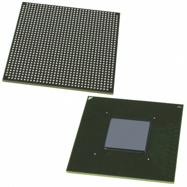
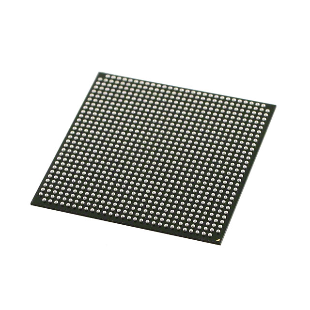
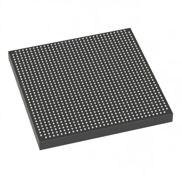
- Package & Mounting 896-BBGA (FCBGA) package; supplier device package listed as 896-FBGA (31×31) with surface-mount assembly.
- Core Supply Operates from a 1.07 V to 1.13 V core voltage range, enabling predictable power provisioning for the programmable core.
- Standards & Compliance RoHS compliant, meeting common environmental governance requirements.
- Documentation Supported by the Arria V device family datasheet covering electrical characteristics, switching characteristics, configuration specifications, and I/O timing.
Typical Applications
- Industrial systems Industrial-grade temperature rating and robust core/I‑O resources suit control, automation, and monitoring equipment.
- I/O‑intensive interfaces 384 I/Os enable wide parallel data buses and multiple simultaneous peripheral connections.
- High‑density logic implementations 190,000 logic elements accommodate complex custom logic, signal processing, and protocol implementation.
- Memory‑heavy designs Large on-chip RAM (13,284,352 bits) supports buffering, packet handling, and lookup/lookup table workloads.
Unique Advantages
- High logic capacity: 190,000 logic elements provide the headroom for complex designs and parallel architectures without immediate redesign.
- Substantial on‑chip RAM: Over 13 million bits of RAM reduce external memory dependency for many buffering and state storage needs.
- Extensive I/O: 384 I/Os simplify integration with wide-data interfaces and multiple peripherals, reducing board-level multiplexing.
- Industrial temperature tolerance: −40°C to 100°C rating enables deployment in temperature-challenging environments common to industrial applications.
- Compact FCBGA package: 896-ball FCBGA (31×31) balances high pin count with a compact footprint for dense board designs.
- Environmentally compliant: RoHS compliance aligns the device with regulatory and sustainability requirements.
Why Choose 5AGXBA5D4F31I5N?
The 5AGXBA5D4F31I5N positions itself as a high-density, industrial-grade Arria V GX FPGA suitable for designs that demand significant logic resources, on-chip RAM, and extensive I/O. Its combination of 190,000 logic elements, more than 13 million RAM bits, and 384 I/Os enables integration of complex, interface-rich functions while maintaining a compact 896-ball FCBGA footprint.
Backed by the Arria V device family documentation for electrical, switching, configuration, and I/O timing details, this device is suited to developers and procurement teams targeting robust, long-lifecycle embedded and industrial FPGA deployments.
Request a quote or submit an inquiry to receive pricing and availability for the 5AGXBA5D4F31I5N.


Date Founded: 1968
Headquarters: Santa Clara, California, USA
Employees: 130,000+
Revenue: $54.23 Billion
Certifications and Memberships: ISO9001:2015, ISO14001:2015, ISO17025:2017, ISO27001:2022, ISO45001:2018, ISO50001:2018


