
5AGXBA7D4F27C5N
| Part Description |
Arria V GX Field Programmable Gate Array (FPGA) IC 336 15470592 242000 672-BBGA, FCBGA |
|---|---|
| Quantity | 683 Available (as of June 15, 2026) |

| Product Category | Field Programmable Gate Array (FPGA) |
|---|---|
| Manufacturer | Intel |
| Manufacturing Status | Obsolete |
| Manufacturer Standard Lead Time | Contact Us |
| Datasheet |
Specifications & Environmental
| Device Package | 672-FBGA (27x27) | Grade | Commercial | Operating Temperature | 0°C – 85°C | ||
|---|---|---|---|---|---|---|---|
| Package / Case | 672-BBGA, FCBGA | Number of I/O | 336 | Voltage | 1.07 V - 1.13 V | ||
| Mounting Method | Surface Mount | RoHS Compliance | RoHS Compliant | REACH Compliance | REACH Unknown | ||
| Moisture Sensitivity Level | 3 (168 Hours) | Number of LABs/CLBs | 11460 | Number of Logic Elements/Cells | 242000 | ||
| Number of Gates | N/A | ECCN | 3A001A2C | HTS Code | 8542.39.0001 | ||
| Qualification | N/A | Total RAM Bits | 15470592 |
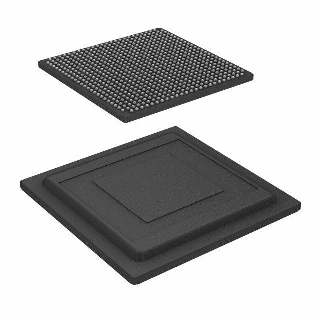
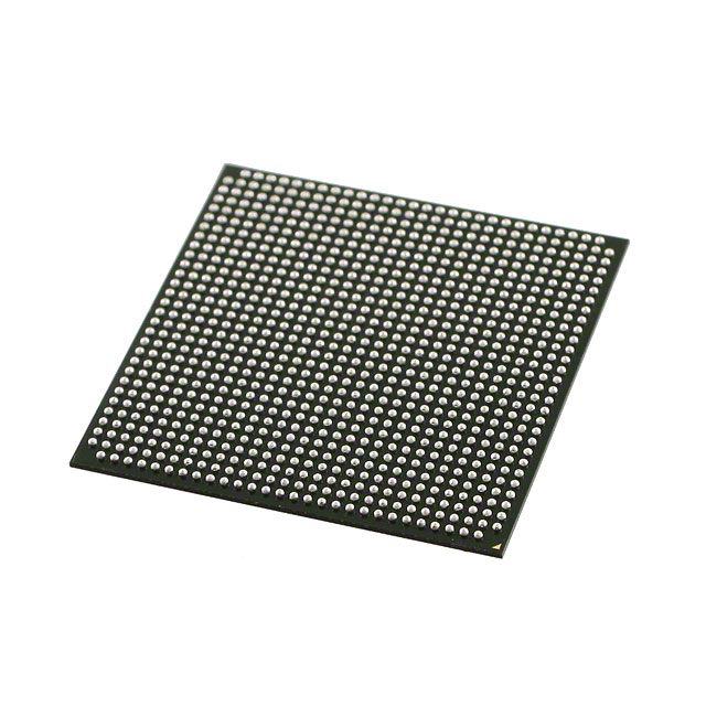
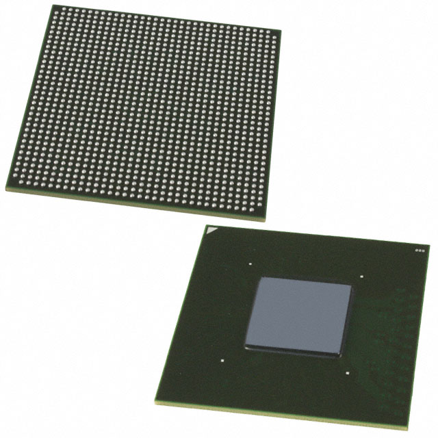
Overview of 5AGXBA7D4F27C5N – Arria V GX Field Programmable Gate Array (FPGA) IC, 672-BBGA (FCBGA)
The 5AGXBA7D4F27C5N is an Intel Arria V GX Field Programmable Gate Array (FPGA) IC supplied in a 672-BBGA FCBGA package. It delivers a high-density programmable fabric with 242,000 logic elements and a large on-chip RAM resource for complex digital designs.
With 336 I/O pins, a compact 672-FBGA (27×27) package, and a documented operating voltage range of 1.07 V to 1.13 V, this commercial-grade device targets system-level designs that require significant logic capacity, on-chip memory, and extensive external interfacing.
Key Features
- Core Logic: 242,000 logic elements provide substantial capacity for implementing complex digital functions and custom accelerators.
- Programmable Fabric Density: 11460 logic array blocks reported at the device level to support partitioning of logic and design modularity.
- On‑Chip Memory: 15,470,592 total RAM bits available for buffering, lookup tables, and state storage within the FPGA fabric.
- I/O Capacity: 336 general-purpose I/O pins for broad external connectivity and interface flexibility.
- Power and Core Voltage: Documented supply range of 1.07 V to 1.13 V for the device core.
- Package and Mounting: 672-BBGA (FCBGA) package — supplier package listed as 672-FBGA (27×27) — designed for surface-mount assembly.
- Operating Range and Grade: Commercial grade device rated for 0 °C to 85 °C operation and RoHS compliant.
- Datasheet Coverage: Supported by the Arria V device datasheet describing electrical characteristics, switching characteristics, configuration specifications, and I/O timing.
Typical Applications
- Custom digital systems: Implement application‑specific logic and accelerators using the device’s large logic and RAM resources.
- I/O‑intensive interfaces: Use the 336 I/O pins to connect multiple peripherals, interfaces, and external memory devices.
- Prototyping and system integration: Rapidly prototype complex designs and validate system behavior with a high-density programmable device.
- Embedded control and data buffering: Leverage on-chip RAM for buffering, state machines, and data-path storage in embedded designs.
Unique Advantages
- High logic capacity: 242,000 logic elements enable implementation of sizeable designs without immediate migration to larger device families.
- Substantial on-chip RAM: Over 15 million RAM bits reduce the need for external memory in many buffering and LUT-based applications.
- Extensive external connectivity: 336 I/Os accommodate multiple peripherals and complex board-level interfaces.
- Compact, manufacturable package: 672-FBGA (27×27) surface-mount package balances density and PCB routing considerations for production boards.
- Commercial temperature suitability: 0 °C to 85 °C rating matches a wide range of standard electronic products and development platforms.
- Standards‑aware supply: RoHS compliance supports regulatory requirements for environmental safety.
Why Choose 5AGXBA7D4F27C5N?
The 5AGXBA7D4F27C5N Arria V GX FPGA provides a combination of high logic density, large on‑chip memory, and a substantial I/O count in a 672‑BBGA FCBGA package, making it well suited for commercial designs that require programmable, high-capacity digital logic. Its documented operating voltage and temperature range, together with the comprehensive Arria V device datasheet, give design teams the technical detail needed for system-level integration and validation.
This device is appropriate for engineers and teams building complex digital subsystems, I/O-rich controllers, and prototype platforms that benefit from a programmable fabric and significant embedded RAM while adhering to commercial temperature and RoHS requirements.
Request a quote or submit an inquiry to receive pricing and availability information for the 5AGXBA7D4F27C5N Arria V GX FPGA.


Date Founded: 1968
Headquarters: Santa Clara, California, USA
Employees: 130,000+
Revenue: $54.23 Billion
Certifications and Memberships: ISO9001:2015, ISO14001:2015, ISO17025:2017, ISO27001:2022, ISO45001:2018, ISO50001:2018


