
5AGXBA7D4F31C4G
| Part Description |
Arria V GX Field Programmable Gate Array (FPGA) IC 384 15470592 242000 896-BBGA, FCBGA |
|---|---|
| Quantity | 1,269 Available (as of June 15, 2026) |

| Product Category | Field Programmable Gate Array (FPGA) |
|---|---|
| Manufacturer | Intel |
| Manufacturing Status | Active |
| Manufacturer Standard Lead Time | 12 Weeks |
| Datasheet |
Specifications & Environmental
| Device Package | 896-FBGA (31x31) | Grade | Commercial | Operating Temperature | 0°C – 85°C | ||
|---|---|---|---|---|---|---|---|
| Package / Case | 896-BBGA, FCBGA | Number of I/O | 384 | Voltage | 1.07 V - 1.13 V | ||
| Mounting Method | Surface Mount | RoHS Compliance | RoHS Compliant | REACH Compliance | REACH Unaffected | ||
| Moisture Sensitivity Level | 3 (168 Hours) | Number of LABs/CLBs | 11460 | Number of Logic Elements/Cells | 242000 | ||
| Number of Gates | N/A | ECCN | PENDING ECCN | HTS Code | 0000.00.0000 | ||
| Qualification | N/A | Total RAM Bits | 15470592 |
Overview of 5AGXBA7D4F31C4G – Arria V GX Field Programmable Gate Array (FPGA) IC
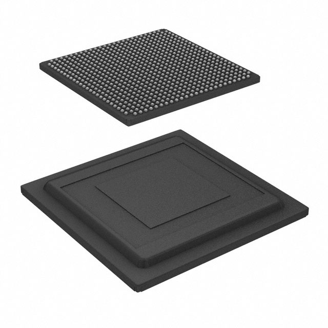
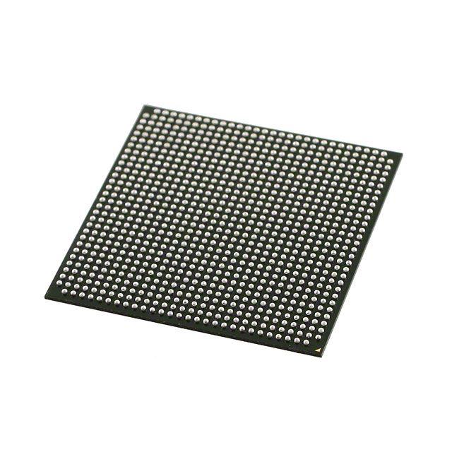
The 5AGXBA7D4F31C4G is an Intel Arria V GX family Field Programmable Gate Array supplied in a 896‑BBGA FCBGA package. It is a commercial‑grade, surface‑mount FPGA offering high logic density, substantial on‑chip RAM, and a large I/O count for complex system designs.
Designed for applications requiring substantial programmable logic and memory integration, this device delivers 242,000 logic elements, 15,470,592 total RAM bits, and 384 I/Os while operating within a core supply window of 1.07 V to 1.13 V and a commercial temperature range of 0 °C to 85 °C.
Key Features
- Core Logic Capacity 242,000 logic elements to implement complex custom logic, state machines, and datapaths.
- On‑Die Memory 15,470,592 total RAM bits for buffering, LUT RAM, FIFOs, and local data storage without immediate dependence on external memory.
- I/O Density 384 user I/Os to support wide interfaces, parallel buses, and high channel counts at the board level.
- Package and Mounting 896‑BBGA, FCBGA package (supplier package: 896‑FBGA, 31×31) in a surface‑mount form factor for high pin count integration.
- Power and Operating Conditions Core voltage range 1.07 V–1.13 V and operating temperature 0 °C–85 °C (commercial grade) to match typical commercial embedded system environments.
- Regulatory RoHS compliant.
Typical Applications
- Data and Packet Processing Large logic capacity and abundant on‑chip RAM enable complex packet parsing, classification, and pipeline implementations.
- Signal and Video Processing High logic density and substantial RAM support parallel processing kernels, buffering, and real‑time frame manipulation.
- Hardware Acceleration and Prototyping The combination of logic elements and I/Os makes the device suitable for accelerating algorithms and validating system architectures on programmable silicon.
- System Integration 384 I/Os and a high‑pin‑count ball grid package facilitate integration with high‑speed peripherals and dense board designs.
Unique Advantages
- Large Logic Resource: 242,000 logic elements support sophisticated, multi‑module designs without excessive partitioning.
- Significant On‑Chip Memory: 15,470,592 RAM bits reduce reliance on external memory for many buffering and caching needs, simplifying board layout.
- Extensive I/O Count: 384 I/Os provide flexibility for parallel interfaces, multi‑lane connections, and dense sensor or peripheral arrays.
- High‑Pin Package in Compact Footprint: 896‑BBGA (31×31) package offers a high pin count while minimizing PCB area impact relative to discrete solutions.
- Tightly Defined Power Window: Core supply specified at 1.07 V–1.13 V supports consistent power provisioning and predictable thermal behavior within the commercial temperature range.
- RoHS Compliant: Meets common environmental directives for commercial electronic products.
Why Choose 5AGXBA7D4F31C4G?
The 5AGXBA7D4F31C4G Arria V GX FPGA targets commercial systems that require a balance of high logic density, on‑chip memory, and abundant I/O in a surface‑mount, high‑pin‑count package. Its specifications—242,000 logic elements, 15,470,592 RAM bits, 384 I/Os, and a defined core voltage window—make it well suited for designers building packet processing, signal processing, acceleration, and complex integration applications.
Backed by the Arria V device documentation, this commercial‑grade FPGA provides a platform for scalable, programmable implementations where integration density and predictable operating conditions are priorities.
Request a quote or submit an inquiry for 5AGXBA7D4F31C4G to receive pricing and availability information for your project requirements.


Date Founded: 1968
Headquarters: Santa Clara, California, USA
Employees: 130,000+
Revenue: $54.23 Billion
Certifications and Memberships: ISO9001:2015, ISO14001:2015, ISO17025:2017, ISO27001:2022, ISO45001:2018, ISO50001:2018


