
5AGXBA7D4F31C5N
| Part Description |
Arria V GX Field Programmable Gate Array (FPGA) IC 384 15470592 242000 896-BBGA, FCBGA |
|---|---|
| Quantity | 369 Available (as of June 14, 2026) |

| Product Category | Field Programmable Gate Array (FPGA) |
|---|---|
| Manufacturer | Intel |
| Manufacturing Status | Obsolete |
| Manufacturer Standard Lead Time | Contact Us |
| Datasheet |
Specifications & Environmental
| Device Package | 896-FBGA (31x31) | Grade | Commercial | Operating Temperature | 0°C – 85°C | ||
|---|---|---|---|---|---|---|---|
| Package / Case | 896-BBGA, FCBGA | Number of I/O | 384 | Voltage | 1.07 V - 1.13 V | ||
| Mounting Method | Surface Mount | RoHS Compliance | RoHS Compliant | REACH Compliance | REACH Unknown | ||
| Moisture Sensitivity Level | 3 (168 Hours) | Number of LABs/CLBs | 11460 | Number of Logic Elements/Cells | 242000 | ||
| Number of Gates | N/A | ECCN | 3A001A2C | HTS Code | 8542.39.0001 | ||
| Qualification | N/A | Total RAM Bits | 15470592 |
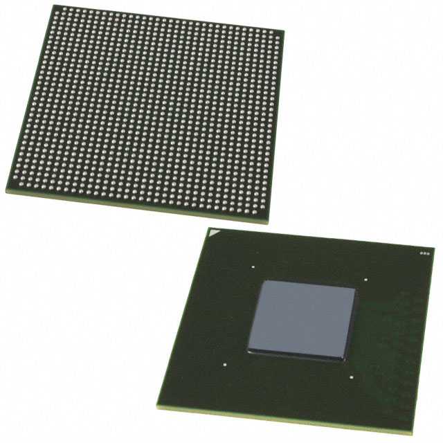
Overview of 5AGXBA7D4F31C5N – Arria V GX FPGA, 896‑BBGA (31×31), 242,000 logic elements
The 5AGXBA7D4F31C5N is an Intel Arria V GX field programmable gate array supplied in a 896‑ball FCBGA package (31×31). This commercial‑grade FPGA delivers a high logic density with 242,000 logic elements and extensive on‑chip memory to support complex, configurable digital designs.
With 384 I/O pins, 15,470,592 total RAM bits, and a tightly specified core supply range, the device is designed for applications that require dense logic, substantial embedded RAM, and a compact surface‑mount package footprint.
Key Features
- Core Logic 242,000 logic elements (LEs) provide high-density programmable logic for complex logic functions and custom hardware acceleration.
- Embedded Memory 15,470,592 total RAM bits of on‑chip memory to support buffering, lookup tables, and data‑intensive kernels.
- I/O Capacity 384 general-purpose I/O pins enable broad interfacing options for external peripherals, memory, and high‑speed I/O subsystems.
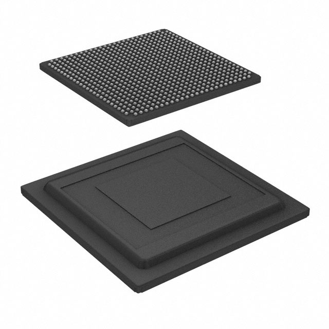
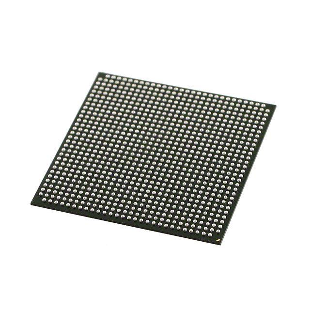
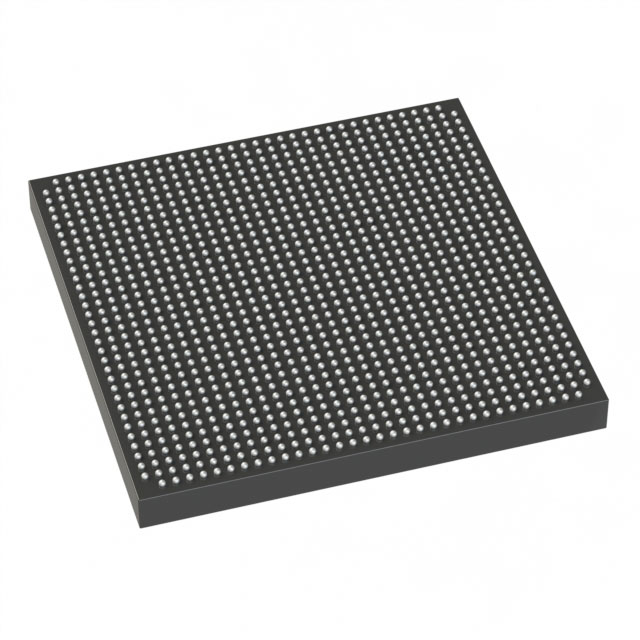
- Package & Mounting 896‑ball BGA (FCBGA) in a 31×31 mm footprint, designed for surface‑mount assembly in compact system designs.
- Power Supply Specified core voltage range of 1.07 V to 1.13 V to support stable core operation and controlled power budgeting.
- Operating Conditions Commercial grade with an operating temperature range of 0 °C to 85 °C for standard temperature environments.
- Standards Compliance RoHS compliant for environmental and manufacturing compatibility.
Typical Applications
- High‑density I/O Systems Use the 384 I/O pins to aggregate and route signals between multiple subsystems, sensors, and external interfaces.
- Embedded Memory‑Intensive Designs Leverage 15,470,592 RAM bits for buffering, packet processing, or large lookup tables within custom logic.
- Custom Logic and Hardware Acceleration Deploy the 242,000 logic elements to implement application‑specific accelerators, protocol engines, or complex state machines.
- Compact Board Designs The 896‑ball FCBGA (31×31) package supports high integration density in space‑constrained PCB layouts.
Unique Advantages
- High logic density: 242,000 logic elements reduce the need for multiple devices, simplifying board-level integration.
- Substantial on‑chip RAM: 15,470,592 total RAM bits enable large buffers and local data storage that improve data throughput and reduce external memory dependence.
- Extensive I/O count: 384 I/O pins allow flexible system partitioning and direct interfacing with multiple peripherals or memory devices.
- Compact BGA package: 896‑ball FCBGA (31×31) supports dense routing and minimized PCB area for compact system designs.
- Tightly specified core voltage: 1.07 V to 1.13 V supply range helps designers plan stable power distribution and thermal profiles.
- Commercial grade and RoHS compliant: Supplies consistent performance across standard commercial operating temperatures while meeting environmental requirements.
Why Choose 5AGXBA7D4F31C5N?
The 5AGXBA7D4F31C5N Arria V GX FPGA combines a high count of logic elements, abundant embedded memory, and broad I/O capability in a compact FCBGA package. It is positioned for engineers who need a configurable, high‑density platform for implementing complex custom logic, embedded buffering, and multi‑interface systems within commercial temperature environments.
Designed for scalable hardware designs, this device offers designers the flexibility to consolidate functions, reduce board complexity, and control BOM cost while relying on Intel’s Arria V device family specifications for power and thermal planning.
Request a quote or submit a procurement inquiry to obtain pricing, availability, and lead‑time information for the 5AGXBA7D4F31C5N Arria V GX FPGA.


Date Founded: 1968
Headquarters: Santa Clara, California, USA
Employees: 130,000+
Revenue: $54.23 Billion
Certifications and Memberships: ISO9001:2015, ISO14001:2015, ISO17025:2017, ISO27001:2022, ISO45001:2018, ISO50001:2018


